Datasheet4U.com
🌙
W170-01 Datasheet | Cypress
Part:
W170-01
Description:
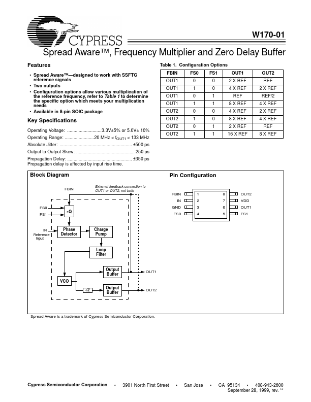
Spread Aware/ Frequency Multiplier and Zero Delay Buffer
Manufacturer:
Cypress
Size:
103.73 KB
W170-01 Datasheet (PDF) Download
Cypress
W170-01
Key Features
Spread Aware™-designed to work with SSFTG reference signals
Available in 8-pin SOIC package Table
×
Close