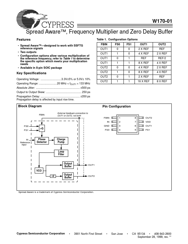
Datasheet4U Logo Datasheet4U.com

W170 - Spread Aware/ Frequency Multiplier and Zero Delay Buffer

Description

Reference Input: The output signals will be synchronized to this signal.

Feedback Input: This input must be fed by one of the outputs (OUT1 or OUT2) to ensure proper functionality.

Features

  • Spread Aware™.
  • designed to work with SSFTG reference signals.
  • Two outputs.
  • Configuration options allow various multiplication of the reference frequency, refer to Table 1 to determine the specific option which meets your multiplication needs.
  • Available in 8-pin SOIC package Table 1. Configuration Options FBIN OUT1 OUT1 OUT1 OUT1 OUT2 OUT2 OUT2 OUT2 FS0 0 1 0 1 0 1 0 1 FS1 0 0 1 1 0 0 1 1 OUT1 2 X REF 4 X REF REF 8 X REF 4 X REF 8 X REF 2 X REF 16 X REF.

📥 Download Datasheet

Datasheet preview – W170

Datasheet Details

Part number W170
Manufacturer Cypress Semiconductor
File Size 103.73 KB
Description Spread Aware/ Frequency Multiplier and Zero Delay Buffer
Datasheet download datasheet W170 Datasheet
Additional preview pages of the W170 datasheet.
Other Datasheets by Cypress Semiconductor

Full PDF Text Transcription

Click to expand full text
W170-01 Spread Aware™, Frequency Multiplier and Zero Delay Buffer Features • Spread Aware™—designed to work with SSFTG reference signals • Two outputs • Configuration options allow various multiplication of the reference frequency, refer to Table 1 to determine the specific option which meets your multiplication needs • Available in 8-pin SOIC package Table 1. Configuration Options FBIN OUT1 OUT1 OUT1 OUT1 OUT2 OUT2 OUT2 OUT2 FS0 0 1 0 1 0 1 0 1 FS1 0 0 1 1 0 0 1 1 OUT1 2 X REF 4 X REF REF 8 X REF 4 X REF 8 X REF 2 X REF 16 X REF OUT2 REF 2 X REF REF/2 4 X REF 2 X REF 4 X REF REF 8 X REF Key Specifications Operating Voltage: ...........................3.3V±5% or 5.0V± 10% Operating Range: .......................20 MHz < fOUT1 < 133 MHz Absolute Jitter: ...................................
Published: |