W182
W182 is Full Feature Peak Reducing EMI Solution manufactured by Cypress.
Feature
Peak Reducing EMI Solution
Features
- Cypress PREMIS™ family offering
- Generates an EMI optimized clocking signal at the output
- Selectable output frequency range
- Single 1.25% or 3.75% down or center spread output
- Integrated loop filter ponents
- Operates with a 3.3 or 5V supply
- Low power CMOS design
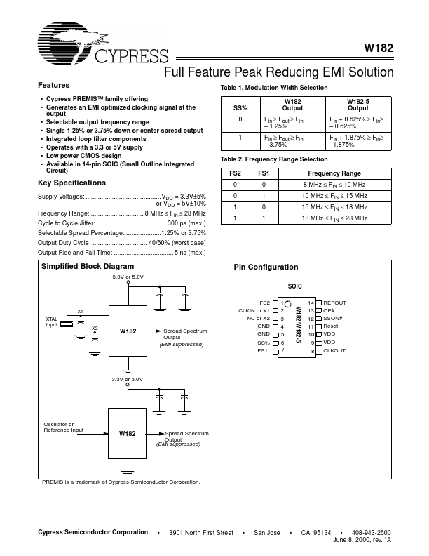
- Available in 14-pin SOIC (Small Outline Integrated Circuit) Table 1. Modulation Width Selection SS% 0 1 W182 Output Fin ≥ Fout ≥ Fin
- 1.25% Fin ≥ Fout ≥ Fin
- 3.75% W182-5 Output Fin + 0.625% ≥ Fin≥
- 0.625% Fin + 1.875% ≥ Fin≥
- 1.875%
Table 2. Frequency Range Selection FS2 0 0 1 1 FS1 0 1 0 1 Frequency Range 8 MHz ≤ FIN ≤ 10 MHz 10 MHz ≤ FIN ≤ 15 MHz 15 MHz ≤ FIN ≤ 18 MHz 18 MHz ≤ FIN ≤ 28 MHz
Key Specifications
Supply Voltages: VDD = 3.3V±5% or VDD = 5V±10% Frequency Range: 8 MHz ≤ Fin ≤ 28 MHz Cycle to Cycle Jitter: 300 ps (max.) Selectable Spread Percentage: 1.25% or 3.75% Output Duty Cycle: 40/60% (worst case) Output Rise and Fall Time: 5 ns (max.)
Simplified Block Diagram
3.3V or 5.0V
Pin Configuration
SOIC FS2 CLKIN or X1 NC or X2 GND GND SS% FS1 1 2 3 4 5 6 14 13 12 11 10 9 8 REFOUT OE# SSON# Reset VDD VDD CLKOUT
W182/W182-5
X1 XTAL Input
X2
Spread Spectrum Output (EMI suppressed)
3.3V or 5.0V
Oscillator or Reference Input
Spread Spectrum Output (EMI suppressed)
PREMIS is a trademark of Cypress Semiconductor Corporation.
Cypress Semiconductor Corporation
- 3901 North First Street
- San Jose
- CA 95134
- 408-943-2600 June 8, 2000, rev.
- A
Pin Definitions
Pin Name CLKOUT REFOUT Pin No. 8 14 Pin Type O O Pin Description
Output Modulated Frequency: Frequency modulated copy of the input clock (SSON# asserted). Non-Modulated Output: This pin provides a copy of the reference frequency. This output will not...