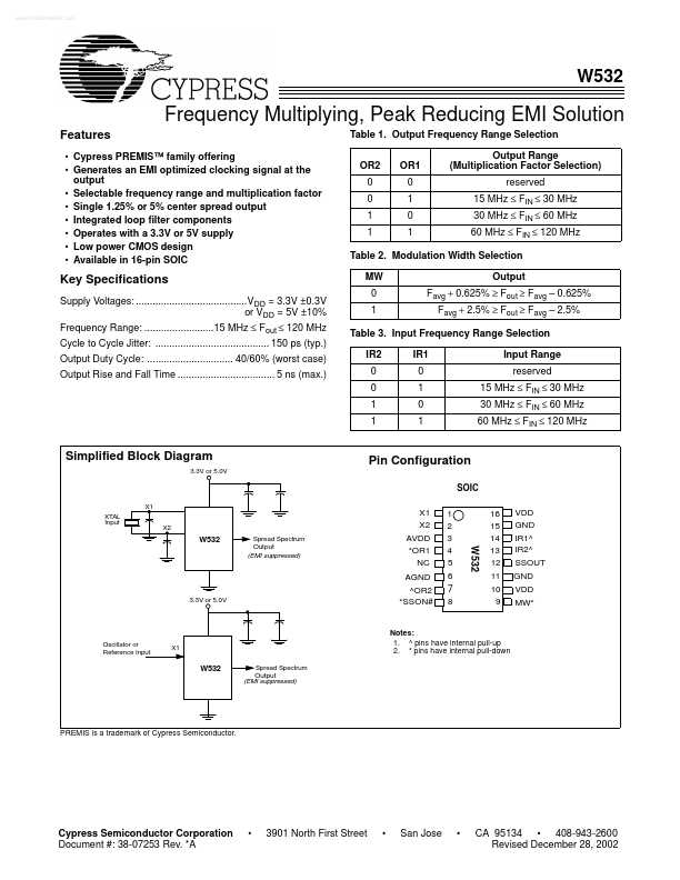
Datasheet4U Logo Datasheet4U.com

W532 - Peak Reducing EMI Solution

Description

Output Modulated Frequency: Frequency modulated signal.

Frequency of the output is selected as shown in Table 1.

Crystal Connection or External Reference Frequency Input: This pin has dual functions.

Features

  • Cypress PREMIS™ family offering.
  • Generates an EMI optimized clocking signal at the output.
  • Selectable frequency range and multiplication factor.
  • Single 1.25% or 5% center spread output.
  • Integrated loop filter components.
  • Operates with a 3.3V or 5V supply.
  • Low power CMOS design.
  • Available in 16-pin SOIC Table 1. Output Frequency Range Selection OR2 0 0 1 1 OR1 0 1 0 1 Output Range (Multiplication Factor Selection) reserved 1.

📥 Download Datasheet

Datasheet preview – W532

Datasheet Details

Part number W532
Manufacturer Cypress Semiconductor
File Size 144.81 KB
Description Peak Reducing EMI Solution
Datasheet download datasheet W532 Datasheet
Additional preview pages of the W532 datasheet.
Other Datasheets by Cypress Semiconductor

Full PDF Text Transcription

Click to expand full text
www.DataSheet4U.com W532 Frequency Multiplying, Peak Reducing EMI Solution Features • Cypress PREMIS™ family offering • Generates an EMI optimized clocking signal at the output • Selectable frequency range and multiplication factor • Single 1.25% or 5% center spread output • Integrated loop filter components • Operates with a 3.3V or 5V supply • Low power CMOS design • Available in 16-pin SOIC Table 1. Output Frequency Range Selection OR2 0 0 1 1 OR1 0 1 0 1 Output Range (Multiplication Factor Selection) reserved 15 MHz ≤ FIN ≤ 30 MHz 30 MHz ≤ FIN ≤ 60 MHz 60 MHz ≤ FIN ≤ 120 MHz Table 2. Modulation Width Selection MW 0 1 Output Favg + 0.625% ≥ Fout ≥ Favg – 0.625% Favg + 2.5% ≥ Fout ≥ Favg – 2.5% Key Specifications Supply Voltages: ........................................VDD = 3.3V ±0.
Published: |