C5002
Overview
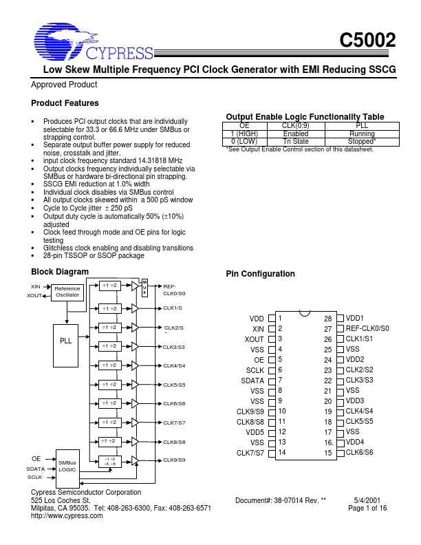
C5002 Low Skew Multiple Frequency PCI Clock Generator with EMI Reducing SSCG Approved Product Product Features § Produces PCI output clocks that are individually selectable for 33.3 or 66.6 MHz und...
| Part | C5002 |
|---|---|
| Description | Low Skew Multiple Frequency PCI Clock Generator |
| Manufacturer | Cypress |
| Size | 122.82 KB |
C5002 Low Skew Multiple Frequency PCI Clock Generator with EMI Reducing SSCG Approved Product Product Features § Produces PCI output clocks that are individually selectable for 33.3 or 66.6 MHz und...
| Part Number | Manufacturer | Description |
|---|---|---|
| C5002 | International | Low Skew Muliple Frequency PCI Clock Generator with EMI Reducing SSCG |
| C5002 | SavantIC | 2SC5002 |
| C5002 | Sanken | 2SC5002 |
| LEF-C5002T | Letex | FULL COLOR LED LAMPS |
| C5001 | International | Low Skew Muliple Frequency PCI Clock Generator with EMI Reducing SSCG |