CY23S08
Overview
- Zero input output propagation delay, adjustable by capacitive load on FBK input
- Multiple configurations (see Available CY23S08 Configurations on page 4)
- Multiple low-skew outputs ❐ 45 ps typical output-output skew (-1) ❐ Two banks of four outputs that can be tristated by two select inputs
- 10 MHz to 140 MHz operating range
- 65 ps typical cycle-to-cycle jitter (-1, -1H)
- Advanced 0.65 m complementary metal oxide semiconductor (CMOS) technology
- Space-saving 16-pin small outline integrated circuit (SOIC) package
- 3.3 V operation
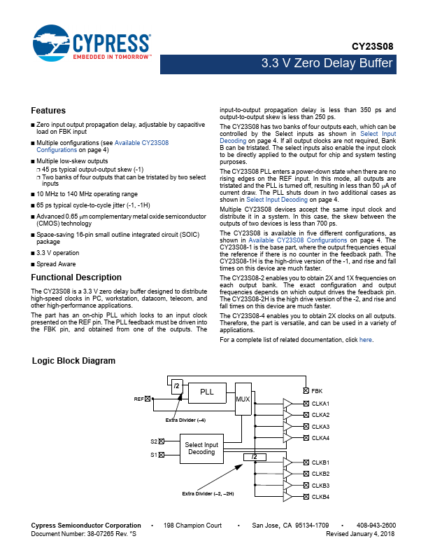
- Spread Aware Functional Description The CY23S08 is a 3.3 V zero delay buffer designed to distribute high-speed clocks in PC, workstation, datacom, telecom, and other high-performance applications. The part has an on-chip PLL which locks to an input clock presented on the REF pin. The PLL feedback must be driven into the FBK pin, and obtained from one of the out