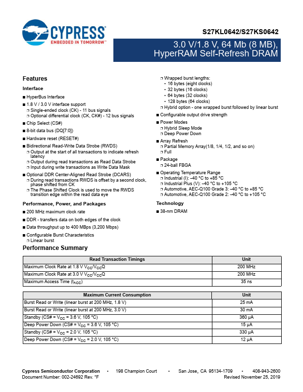
Datasheet4U Logo Datasheet4U.com

S27KS0642 - HyperRAM Self-Refresh DRAM

This page provides the datasheet information for the S27KS0642, a member of the S27KL0642 HyperRAM Self-Refresh DRAM family.

Description

4 HyperBus Interface 4 Product Overview 6 HyperBus Interface 6 Signal Description 7 Input/Output Summary 7 HyperBus Transaction Details 8 Command/Address Bit Assignments 8 Read Transactions 12 Write Transactions (Memory Array Write) 13 Write Transactions without Initial Latency (Register W

Features

  • Interface.
  • HyperBus Interface.
  • 1.8 V / 3.0 V interface support.
  • Single-ended clock (CK) - 11 bus signals.
  • Optional differential clock (CK, CK#) - 12 bus signals.
  • Chip Select (CS#).
  • 8-bit data bus (DQ[7:0]).
  • Hardware reset (RESET#).
  • Bidirectional Read-Write Data Strobe (RWDS).
  • Output at the start of all transactions to indicate refresh latency.
  • Output during read transactions as Read Data Strobe.
  • Input during write transactions as Write Data.

📥 Download Datasheet

Datasheet preview – S27KS0642

Datasheet Details

Part number S27KS0642
Manufacturer Cypress
File Size 1.17 MB
Description HyperRAM Self-Refresh DRAM
Datasheet download datasheet S27KS0642 Datasheet
Additional preview pages of the S27KS0642 datasheet.
Other Datasheets by Cypress

Full PDF Text Transcription

Click to expand full text
S27KL0642/S27KS0642 3.0 V/1.8 V, 64 Mb (8 MB), HyperRAM Self-Refresh DRAM S27KL0642/S27KS0642, 3.0 V/1.8 V, 64 Mb (8 MB), HyperRAM Self-Refresh DRAM Features Interface ■ HyperBus Interface ■ 1.8 V / 3.
Published: |