• Part: BD429A
  • Description: Line Driver
  • Manufacturer: DEI
  • Size: 596.17 KB
Download BD429A Datasheet PDF
DEI
BD429A
BD429A is Line Driver manufactured by DEI.
- Part of the BD429B comparator family.
Features : - - - - - - - - - - - - ARINC 429 Line Driver for HI speed (100 k Hz) and LOW speed (12.5 k Hz) data rates Pin for Pin replacement part for industry standard ARINC 429 Line Drivers Available in a 16 Pin SOIC (WB), 16 Pin CERDIP, 16 Pin Plastic Dip, 16 Lead Ceramic SOP, 28L CLCC and 28L PLCC Low EMI RS-422 line driver mode for data rates up to 100 k Hz Adjustable slew rates via two external capacitors Inputs are TTL and CMOS patible Low quiescent power of 125m W (typical) Programmable output differential range via VREF pin Outputs are fused for failsafe overvoltage protection Drives full ARINC load of 400Ω and 30,000p F Extended (-55°C/+85°C) and Military (-55°C/+125°C) temperature ranges 100% Final Testing Figure 1: BD429 Block Diagram © 2008 Device Engineering Incorporated Page 2 of 14 DS-MW-00429-01 Rev. C 8/1/08 General Description : 
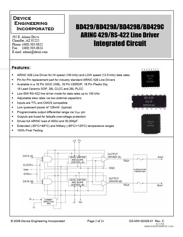
The BD429 ARINC Line Driver Circuit is a bipolar monolithic IC designed to meet the requirements of several general aviation serial data bus standards. These include the differential bipolar RZ types such as ARINC 429, ARINC 571, and ARINC 575, as well as the differential NRZ types such as the RS-422 standard. Functional Description : Modes: The BD429 operates in either a 429 mode or a 422 mode as controlled by the 429/422´ pin. 429 Mode: In 429 mode, the serial data is presented on the DATA(A) and DATA(B) inputs in the dual rail format defined in the MARK 33 Digital Information Transfer System - ARINC Specification 429-10. The driver is enabled by the SYNC and CLOCK inputs. The output voltage level is programmed by the VREF input and is normally tied to +5VDC along with V1 to produce output levels of +5 volts, 0 volts, and - 5 volts on each output for ±10 volts differential outputs. - See Figure 4. .. 422 Mode: In 422 mode, the serial data is presented on DATA(A) input. The driver is enabled by the SYNC and CLOCK inputs. The outputs swings between 0 volts and +5 volts if VREF is at +5VDC. - See Figure 5. Output Resistance:...