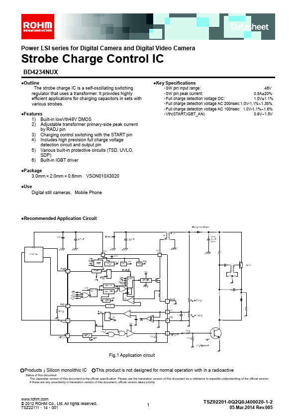
BD4234NUX Overview
(UNIT:mm) Pin No. Pin Name 1 PGND 2 IGBT_OUT 3 GND 4 VC 5 VCC 6 START 7 IGBT_IN 8 RADJ 9 FULL 10 SW Function Power GND IGBT Driver output pin GND pin Full charge detection pin VCC supply pin Charge start signal input pin IGBT Driver output start signal input.
BD4234NUX Key Features
- Key Specifications
- SW pin input range
- SW pin peak current
- Full charge detection voltage DC
- Full charge detection voltage AC 200nsec:1.0V-1.1%~1.35%
- Full charge detection voltage AC 100nsec: 1.0V-1.1%~1.6%
- Vth(START,IGBT_AN)
- Package 3.0mm×2.0mm×0.6mm VSON010X3020
- Use Digital still cameras、Mobile Phone
- Remended Application Circuit
BD4234NUX Applications
- Features 1) Built-in lowVth48V DMOS 2) Adjustable transformer primary-side peak current by RADJ pin 3) Charging control switching with the START pin 4) Includes