PI6CB33202
PI6CB33202 is Very-Low-Power Two-Output PCIe Clock Buffer manufactured by Diodes Incorporated.
Features
Description yy 3.3V Supply Voltage yy HCSL Input: 100MHz; Also supports 50MHz, 125MHz, or
133.33MHz via SMBus yy Two Differential Low-Power HCSL Outputs with On-Chip
Termination yy Default ZOUT = 85Ω yy Spread Spectrum Tolerant yy Individual Output Enable yy Programmable Slew Rate and Output Amplitude for Each
Output yy Differential Outputs Blocked until PLL is Locked yy Strapping Pins or SMBus for Configuration yy Differential output-to-output skew <50ps yy Very low jitter outputs
ààDifferential cycle-to-cycle jitter <50ps ààPCIe Gen1/Gen2/Gen3/Gen4/Gen5 CC pliant ààPCIe Gen 2 and 3 SRi S and SRn S pliant yy Totally Lead-Free & Fully Ro HS pliant (Notes 1 & 2) yy Halogen and Antimony Free. “Green” Device (Note 3) yy For automotive applications requiring specific change control (i.e. parts qualified to AEC-Q100/101/104/200, PPAP capable, and manufactured in IATF 16949 certified facilities), please contact us or your local Diodes representative. https://.diodes./quality/product-definitions/ yy Packaging (Pb-free & Green): àà24-lead 4mm × 4mm TQFN
The PI6CB33202 is a two-output very-low-power PCIe Gen1/ Gen2/Gen3/Gen4/Gen5 clock buffer. It takes a reference input to fan out two 100MHz low-power differential HCSL outputs with on-chip terminations. The on-chip termination can save eight external resistors and make layout easier. Individual OE pin for each output provides easier power management.
It uses Diodes proprietary PLL design to achieve very-low jitter that meets PCIe Gen1/Gen2/Gen3/Gen4/Gen5 requirements. Other than PCIe 100MHz support, this device also support Ethernet application with 50MHz, 125MHz, and 133.33MHz via SMBus. It provides various options such as different slew rate and amplitude through SMBUS, so users can configure the device easily to get the optimized performance for their individual boards.
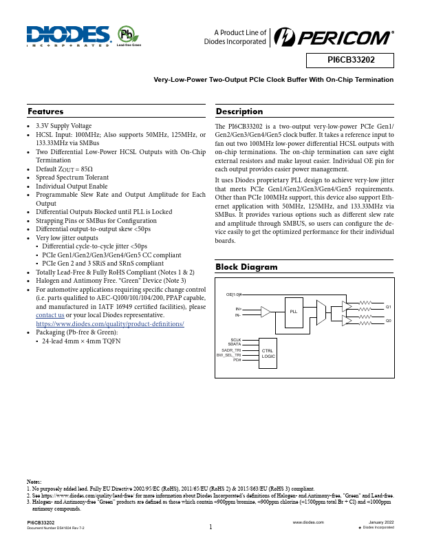
Block Diagram
OE[1:0]#
IN+ IN-
Q1
Q0
SCLK SDATA
SADR_TRI BW_SEL_TRI
PD#
CTRL LOGIC
Notes: 1. No purposely added lead. Fully EU...