Datasheet4U Logo Datasheet4U.com

3D3612 - 8-BIT & 12-BIT PROGRAMMABLE PULSE GENERATORS

Download the 3D3612 datasheet PDF. This datasheet also covers the 3D3608 variant, as both devices belong to the same 8-bit & 12-bit programmable pulse generators family and are provided as variant models within a single manufacturer datasheet.

Description

The 3D3608 & 3D3612 devices are versatile 8- & 12-bit programmable monolithic pulse generators.

A rising-edge on the trigger input (TRIG) initiates the pulse, which is presented on the output pins (OUT,OUTB).

Features

  • All-silicon, low-power CMOS technology 3.3V operation Vapor phase, IR and wave solderable Programmable via latched parallel interface Increment range: 0.25ns through 800us Pulse width tolerance: 1% (See Table 1) Supply current: 8mA typical Temperature stability: ±1.5% max (-40C to 85C) Vdd stability: ±1.0% max (3.0V to 3.6V) TRIG RES P0 P2 P4 P6 NC GND 1 2 3 4 5 6 7 8 16 15 14 13 12 11 10 9 data 3 delay de.

📥 Download Datasheet

Note: The manufacturer provides a single datasheet file (3D3608_DataDelayDevices.pdf) that lists specifications for multiple related part numbers.

Datasheet Details

Part number 3D3612
Manufacturer Data Delay Devices
File Size 375.97 KB
Description 8-BIT & 12-BIT PROGRAMMABLE PULSE GENERATORS
Datasheet download datasheet 3D3612 Datasheet

Full PDF Text Transcription (Reference)

The following content is an automatically extracted verbatim text from the original manufacturer datasheet and is provided for reference purposes only.

View original datasheet text
3D3608 & 3D3612 8-BIT & 12-BIT PROGRAMMABLE PULSE GENERATORS (SERIES 3D3608 & 3D3612: PARALLEL INTERFACE) FEATURES • • • • • • • • • All-silicon, low-power CMOS technology 3.3V operation Vapor phase, IR and wave solderable Programmable via latched parallel interface Increment range: 0.25ns through 800us Pulse width tolerance: 1% (See Table 1) Supply current: 8mA typical Temperature stability: ±1.5% max (-40C to 85C) Vdd stability: ±1.0% max (3.0V to 3.6V) 
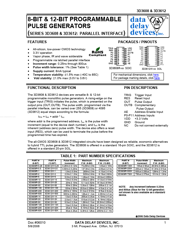
TRIG RES P0 P2 P4 P6 NC GND 1 2 3 4 5 6 7 8 16 15 14 13 12 11 10 9 data 3 delay devices, inc. VDD OUT OUTB P1 P3 P5 P7 AE TRIG RES P0 P2 P4 P6 P8 NC P10 GND 1 2 3 4 5 6 7 8 9 10 20 19 18 17 16 15 14 13 12 11  PACKAGES / PINOUTS VDD OUT OUTB P1 P3 P5 P7 P9 AE P11 3D3608R-xx SOIC 3D3612W-xx SOL For mechanical dimensions, click here.
Published: |