DP170N03
DP170N03 is N-Channel MOSFET manufactured by Developer Microelectronics.
Description
Single N Channel Enhancement Power MOSFET
Product Summary
DP170N03 uses advanced trench technology to provide excellent RDS(ON), low gate charge with a 20V gate rating. This device is suitable for use as a load switch or in PWM applications.
VDS ID (at VGS=20V) RDS(ON) (at VGS = 10V) RDS(ON) (at VGS = 4.5V)
30 V 13A < 10.5mΩ < 12mΩ
- Ro HS and Halogen-Free plaint
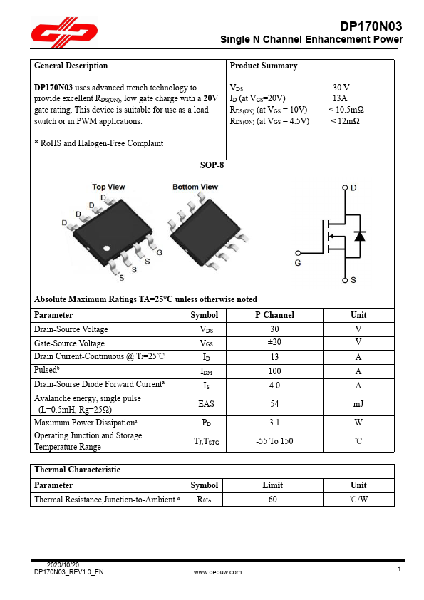
SOP-8
Absolute Maximum Ratings TA=25°C unless otherwise noted
Parameter
Symbol
P-Channel
Drain-Source Voltage
Gate-Source Voltage Drain Current-Continuous @ TJ=25℃ Pulsedb Drain-Sourse Diode Forward Currenta
Avalanche energy, single pulse (L=0.5m H, Rg=25Ω) Maximum Power Dissipationa Operating Junction and Storage Temperature Range
VDS VGS ID IDM IS
TJ,TSTG
30 ±20 13 100 4.0
-55 To 150
Thermal Characteristic Parameter Thermal Resistance,Junction-to-Ambient a
Symbol RθJA
Limit 60
Unit V V A A A m J W ℃
Unit ℃/W
2020/10/20 DP170N03_REV1.0_EN
.depuw....