Overview: ç Prev Page
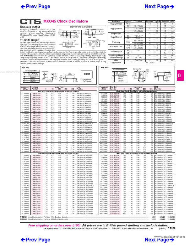
MXO45 Clock Oscillators
Standard Output
• Frequency Tolerance: ±100ppm, 0°C ~ 70°C • CMOS patible • Fully hermetically-sealed package • 8/14-pin patible • Drives up to 10 standard TTL Loads • Input Voltage: +5V DC ± .5V
V0H
1 Next Page è
Parameter Supply Voltage Supply Current Output Load Output Current
Test
A Symbol VCC ICC — — — IOH IOH Duty Tr/Tf Tr/Tf VIH VIL Cin Iz — Condition — 1.0 ~ 7.0MHz >7.0 ~ 25MHz >25 ~ 50MHz — VOH= 3.9V VOH= 0.4V 1.0 ~ 50MHz >50 ~ 70MHz 1.0 ~ 25MHz >25 ~ 70MHz — — — VIL= 0.8V Peak-Peak Minimum Typical 4.5 — — — — — — 45 40 — — 2 — — — — 0°C ~ 70°C 5 5 15 30 — — — — — 5 3 — — — — 30 Maximum Units 5.5 12 25 40 10 -16 16 55 60 8 5 — 0.8 10 0.05 50 V mA mA mA TTL mA mA % % ns ns V V pF mA ps Wave Form Conditions
V0H 90% Vdd 10% Vdd T1 T2 TF T1 - Rise Time T2 - Fall Time /2 Vdd V0L TR 2.4V 0.4V GND TR 1.4V V0L T1 T2 TF Tri-State Output 14 Test 14 8 RL 390 A OSC Tri-State Logic uses the two standard logic levels of 15 VDC .01 OSC V .01 VDC 15 pF V high (logic 1) and low (logic 0) but has added a third 7 pF μf μf 7 7 state that is not a logic level but an open circuit conDiode: 1N4148 CMOS dition that effectively disconnects the output from TTL your circuit with a high impedance (floating) state, thereby enabling the use of numerous oscillators on the same bus line. Also, by using the enable pin to control the output, the crystal is still running even when the output is disabled (stand-by mode), thus eliminating any start-up time for the oscillator. CTS HCMOS/TTL products utilize an Application Specific Integrated Circuit (ASIC) design strategy. Employing a single design family supporting both HCMOS/TTL applications helps in reducing costs and lead times. Utilizing ASIC technology reduces the number of ponents inside the XO (crystal oscillator), thus increasing reliability and further reducing cost.