74AUP1G125
74AUP1G125 is SINGLE BUFFER GATE manufactured by Diodes Incorporated.
SINGLE BUFFER GATE WITH 3-STATE OUTPUT
Description
The Advanced, Ultra Low Power (AUP) CMOS logic family is designed for low power and extended battery life in portable applications.
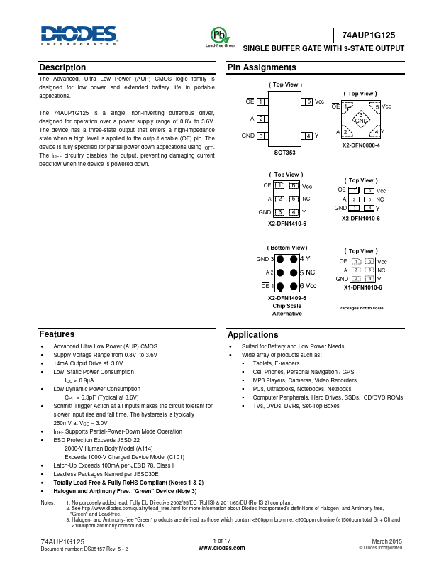
Pin Assignments
The 74AUP1G125 is a single, non-inverting buffer/bus driver, designed for operation over a power supply range of 0.8V to 3.6V. The device has a three-state output that enters a high-impedance state when a high level is applied to the output enable (OE) pin. The device is fully specified for partial power down applications using IOFF. The IOFF circuitry disables the output, preventing damaging current backflow when the device is powered down.
Features
- Advanced Ultra Low Power...