Diodes Incorporated BS250
P-CHANNEL ENHANCEMENT MODE DMOS TRANSISTOR
| Part No. | BS250 |
|---|---|
| Datasheet | BS250 Download |
| Manufacturer |  Diodes Incorporated |
| Description | P-CHANNEL ENHANCEMENT MODE DMOS TRANSISTOR |
| Buy | Stock & Price |
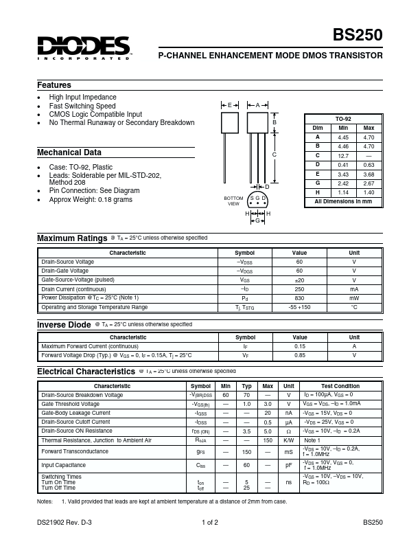
FEATURES
●●
●
● High Input Impedance Fast Switching Speed CMOS Logic Compatible Input No Thermal Runaway or Secondary Breakdown E A B TO-92 Dim A B Min 4.45 4.46 12.7 0.41 3.43 2.42 1.14 Max 4.70 4.70 — 0.63 3.68 2.67 1.40
MECHANICAL DATA
●●
●
● Case: TO-92, Plastic Leads: Solderable per MIL-STD-202, Method 208 Pin Connection: See Diagram Approx Weight: 0.18 grams C C D E G H D BOTTOM VIEW SG D All Dimensions in mm H G H
MAXIMUM RATINGS
Drain-Source Voltage Drain-Gate Voltage @ TA = 25°C unless otherwise specified Characteristic Symbol –VDSS –VDGS VGS –ID Pd Tj, TSTG Value 60 60 ±20 250 830 -55 +150 Unit V V V mA mW °C Gate-Source-Voltage (pulsed) Drain Current (continuous) Power Dissipation @TC = 25°C (Note 1) Operating and Storage Temperature Range Inverse Diode @ TA = 25°C unless otherwise specified Characteristic Symbol IF VF Value 0.15 0.85 Unit A V Maximum Forward Current (continuous) Forward Voltage Drop (Typ.) @ VGS = 0, IF = 0.15A, Tj = 25°CELECTRICAL CHARACTERISTICS
Charac...