DMP1011UCB9
Description
This 3rd generation Lateral MOSFET (LD-MOS) is engineered to minimize on-state losses and switch ultra-fast, making it ideal for high-efficiency power transfer. It uses Chip-Scale Package (CSP) to increase power density by bining low thermal impedance with minimal RDS(ON) per footprint area.
Key Features
- LD-MOS Technology with the Lowest Figure of Merit: -RDS(ON) = 8.2mΩ to Minimize On-State Losses -Qg = 8.1nC for Ultra-Fast Switching
- VGS(th) = -0.8V Typ. for a Low Turn-On Potential
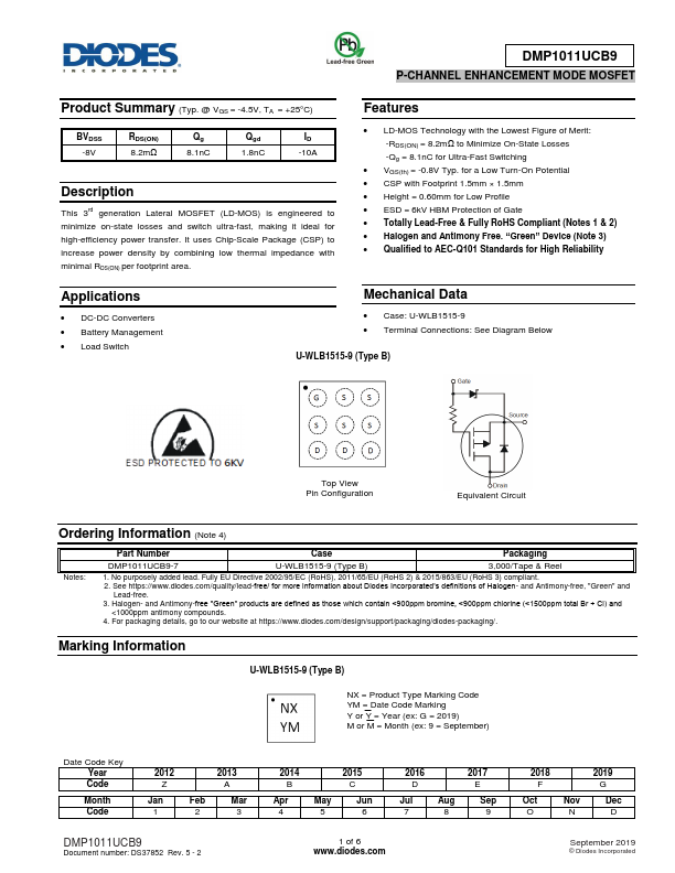
- CSP with Footprint 1.5mm × 1.5mm
- Height = 0.60mm for Low Profile
- ESD = 6kV HBM Protection of Gate
- Totally Lead-Free & Fully RoHS compliant (Notes 1 &
- Halogen and Antimony Free. “Green” Device (Note
- Qualified to AEC-Q101 Standards for High Reliability