DMP2200UDW
DMP2200UDW is P-Channel MOSFET manufactured by Diodes Incorporated.
ADVANCE INFORMATION
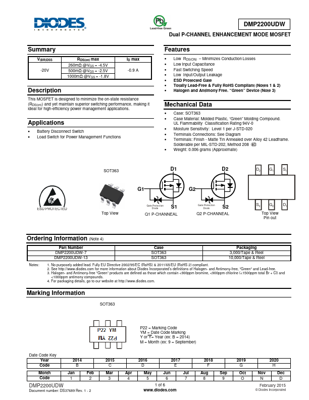
Summary
V(BR)DSS -20V
RDS(on) max 260mΩ @VGS = -4.5V 500mΩ @VGS = -2.5V 1000mΩ @VGS = -1.8V
ID max -0.9 A
Description
This MOSFET is designed to minimize the on-state resistance (RDS(on)) and yet maintain superior switching performance, making it ideal for high-efficiency power management applications.
Applications
- Battery Disconnect Switch
- Load Switch for Power Management Functions
Dual P-CHANNEL ENHANCEMENT MODE MOSFET
Features
- Low RDS(ON)
- Minimizes Conduction Losses
- Low Input Capacitance
- Fast Switching Speed
- Low Input/Output Leakage
- ESD Protected Gate
- Totally Lead-Free & Fully RoHS pliant (Notes 1 & 2)
- Halogen and Antimony...