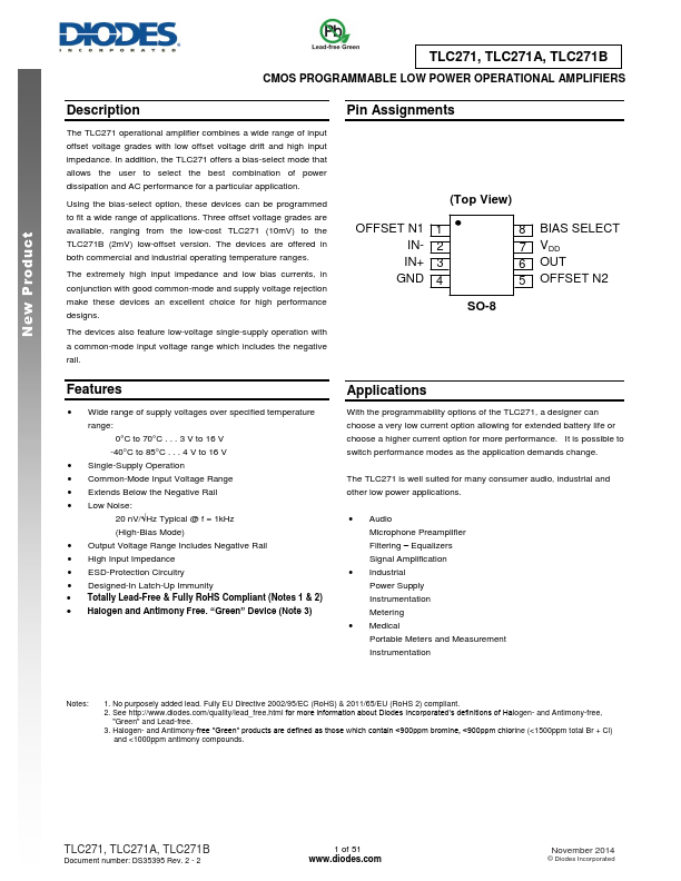
Datasheet4U Logo Datasheet4U.com

TLC271 - CMOS PROGRAMMABLE LOW POWER OPERATIONAL AMPLIFIERS

General Description

The TLC271 operational amplifier combines a wide range of input offset voltage grades with low offset voltage drift and high input impedance.

Key Features

  • Wide range of supply voltages over specified temperature range: 0°C to 70°C . . . 3 V to 16 V -40°C to 85°C . . . 4 V to 16 V.
  • Single-Supply Operation.
  • Common-Mode Input Voltage Range.
  • Extends Below the Negative Rail.
  • Low Noise: 20 nV/√Hz Typical @ f = 1kHz (High-Bias Mode).
  • Output Voltage Range Includes Negative Rail.
  • High Input Impedance.
  • ESD-Protection Circuitry.
  • Designed-In Latch-Up Immunity.
  • Totally Lead-Free & Fully RoHS Compliant (Notes 1.

📥 Download Datasheet

Full PDF Text Transcription (Reference)

The following content is an automatically extracted verbatim text from the original manufacturer datasheet and is provided for reference purposes only.

View original datasheet text
New Product TLC271, TLC271A, TLC271B CMOS PROGRAMMABLE LOW POWER OPERATIONAL AMPLIFIERS Description The TLC271 operational amplifier combines a wide range of input offset voltage grades with low offset voltage drift and high input impedance. In addition, the TLC271 offers a bias-select mode that allows the user to select the best combination of power dissipation and AC performance for a particular application. Using the bias-select option, these devices can be programmed to fit a wide range of applications. Three offset voltage grades are available, ranging from the low-cost TLC271 (10mV) to the TLC271B (2mV) low-offset version. The devices are offered in both commercial and industrial operating temperature ranges.