DFD2N60
DFD2N60 is N-Channel MOSFET manufactured by DnI.
Features
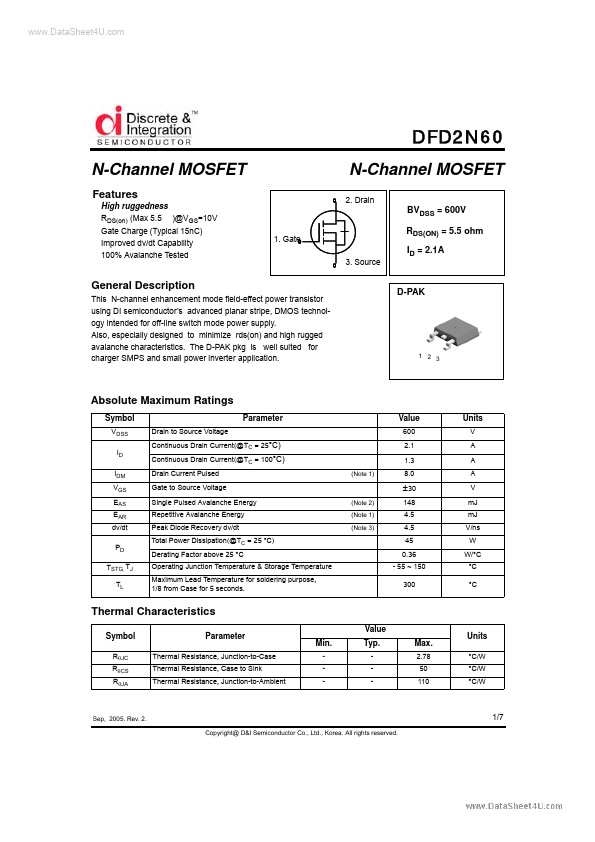
High ruggedness RDS(on) (Max 5.5 )@VGS=10V Gate Charge (Typical 15n C) Improved dv/dt Capability 100% Avalanche Tested 1. Gate {
{ {
N-Channel MOSFET
2. Drain
BVDSS = 600V RDS(ON) = 5.5 ohm ID = 2.1A
3. Source
General Description
This N-channel enhancement mode field-effect power transistor using DI semiconductor’s advanced planar stripe, DMOS technology intended for off-line switch mode power supply. Also, especially designed to minimize rds(on) and high rugged avalanche characteristics. The D-PAK pkg is well suited for charger SMPS and small power inverter application.
D-PAK
1 2 3
Absolute Maximum Ratings
Symbol
VDSS ID IDM VGS EAS EAR dv/dt PD TSTG, TJ TL Drain to Source Voltage Continuous Drain Current(@TC = 25°C) Continuous Drain Current(@TC = 100°C) Drain Current Pulsed Gate to Source Voltage Single Pulsed Avalanche Energy Repetitive Avalanche Energy Peak Diode Recovery dv/dt Total Power Dissipation(@TC = 25 °C) Derating Factor above 25 °C Operating Junction Temperature & Storage Temperature Maximum Lead Temperature for soldering purpose, 1/8 from Case for 5 seconds.
(Note 2) (Note 1) (Note 3) (Note 1)
Parameter
Value
600 2.1 1.3 8.0
Units
V A A A V m J m J V/ns W W/°C °C °C
±30
148 4.5 4.5 45 0.36
- 55 ~ 150 300
Thermal Characteristics
Symbol
RθJC RθCS RθJA
Parameter
Thermal Resistance, Junction-to-Case Thermal Resistance, Case to Sink Thermal Resistance, Junction-to-Ambient
Value Min.
- Typ.
- Max.
2.78 50 110
Units
°C/W °C/W °C/W
Sep, 2005. Rev. 2. Copyright@ D&I Semiconductor Co., Ltd., Korea. All rights reserved.
1/7
..
Electrical Characteristics
Symbol Off Characteristics
BVDSS BVDSS/ TJ IDSS Drain-Source Breakdown Voltage Breakdown Voltage Temperature coefficient Drain-Source Leakage Current Gate-Source Leakage, Forward Gate-source Leakage, Reverse VGS = 0V, ID = 250u A ID = 250u A, referenced to 25 °C VDS = 600V, VGS = 0V VDS = 480V, TC = 125 °C VGS = 30V, VDS = 0V VGS = -30V, VDS = 0V VDS = VGS, ID = 250u A VGS =10 V,...