F59L4G81KA Overview
Description
The device has 4352-byte static registers which allow program and read data to be transferred between the register and the memory cell array in 4352-byte increments. The Erase operation is implemented in a single block unit (256Kbytes + 16Kbytes).
Key Features
- Voltage Supply VCC: 3.3V (2.7 V ~ 3.6V)
- Organization Page Size: (4K +
- bytes Data Register: (4K +
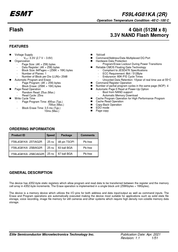
- bytes Block Size: 64Pages = (256K + 16K) bytes Number of Planes: 1 Number of Block per Die (LUN)= 2048
- Automatic Program and Erase Page Program: (4K +
- bytes Block Erase: (256K + 16K) bytes
- Page Read Operation Random Read: 25us (Max.) Read Cycle: 25ns
- 3.3V NAND Flash Memory
- Command/Address/Data Multiplexed DQ Port
- Hardware Data Protection Program/Erase Lockout During Power Transitions