Datasheet4U.com
🌙
55N03L Datasheet | Unknown Manufacturer
Part:
55N03L
Description:
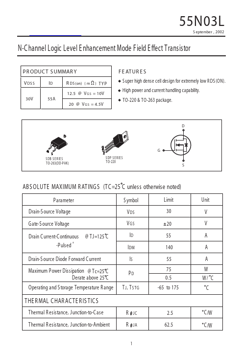
N-Channel FET
Manufacturer:
Unknown Manufacturer
Size:
234.38 KB
55N03L Datasheet (PDF) Download
Unknown Manufacturer
55N03L
Key Features
50 -25 0 25 50 75 100 125
×
Close