74LS107 Overview
Key Specifications
Description
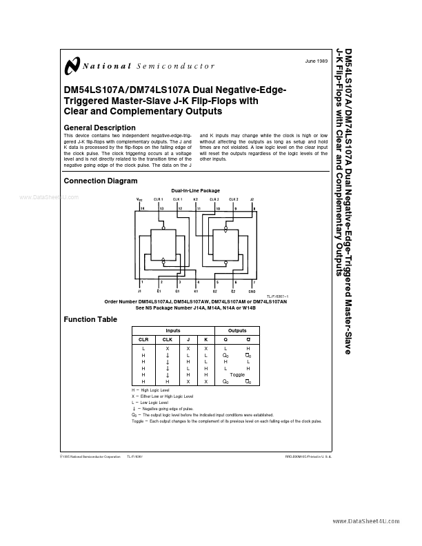
This device contains two independent negative-edge-triggered J-K flip-flops with complementary outputs The J and K data is processed by the flip-flops on the falling edge of the clock pulse The clock triggering occurs at a voltage level and is not directly related to the transition time of the negative going edge of the clock pulse The data on the J and K inputs may change while the clock is high or low without affecting the outputs as long as setup and hold times are not violated A low logic level on the clear input will reset the outputs regardless of the logic levels of the other inputs Connection Diagram Dual-In-Line Package TL F 6367 – 1 Order Number DM54LS107AJ DM54LS107AW DM74LS107AM or DM74LS107AN See NS Package Number J14A M14A N14A or W14B Function Table Inputs CLR L H H H H H CLK X J X L H L H X K X L L H H X Q L Q0 H L Toggle Q0 Q0 Outputs Q H Q0 L H v v v v H H e High Logic Level X e Either Low or High Logic Level L e Low Logic Level v e Negative going edge of pulse Q0 e The output logic level before the indicated input conditions were established Toggle e Each output changes to the complement of its previous level on each falling edge of the clock pulse C1995 National Semiconductor Corporation TL F 6367 RRD-B30M105 Printed in U S A If Military Aerospace specified devices are required please contact the National Semiconductor Sales Office Distributors for availability and specifications Supply Voltage 7V Input Voltage 7V Operating Free Air Temperature Range b 55 C to a 125 C DM54LS DM74LS 0 C to a 70 C b 65 C to a 150 C Storage Temperature Range Note The ‘‘.