Datasheet Summary
Jan 2003
AO9926A Dual N-Channel Enhancement Mode Field Effect Transistor
General Description
The AO9926A uses advanced trench technology to provide excellent RDS(ON) and low gate charge. They offer operation over a wide gate drive range from 1.8V to 8V. The two devices may be used individually, in parallel or to form a bidirectional blocking switch.
Features
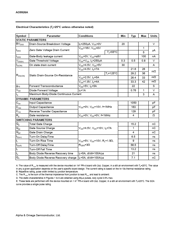
VDS (V) = 20V ID = 7A RDS(ON) < 26m Ω (VGS = 4.5V) RDS(ON) < 33m Ω (VGS = 2.5V) RDS(ON) < 42m Ω (VGS = 1.8V)
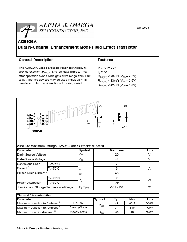
D1 S2 G2 S1 G1 1 2 3 4 8 7 6 5 D2 D2 D1 D1
D2
G1 S1
G2...