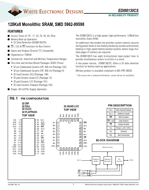
EDI88130CS Description
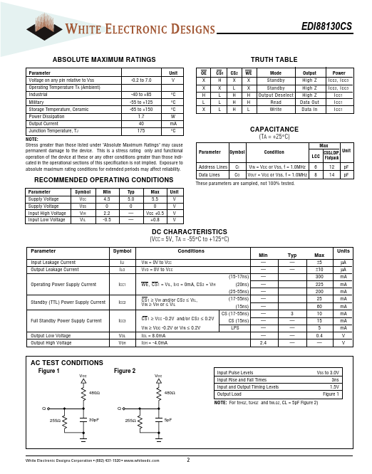
10 1 White Electronic Designs Corporation (602) 437-1520 .whiteedc. Stress greater than those listed under " Ratings" may cause permanent damage to the device. This is a stress rating only and functional operation of the device at these or any other conditions grea.
EDI88130CS Key Features
- 2V Data Retention (EDI88130LPS) s CS1, CS2 & OE Functions for Bus Control s Inputs and Outputs Directly TTL patible s Or
EDI88130CS Applications
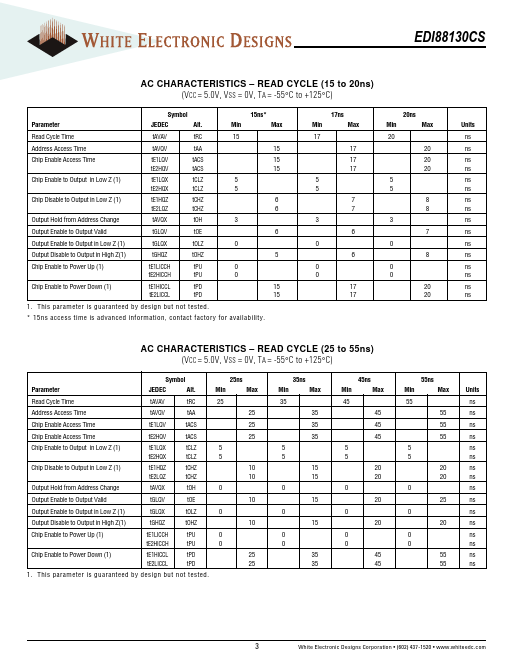
- 15ns access time is advanced information, contact factory for availability