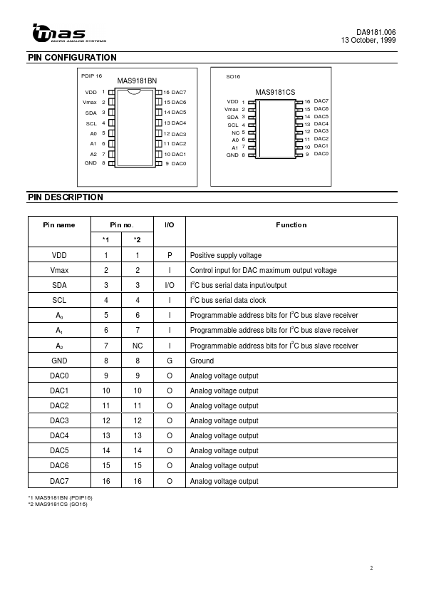
MAS9181BN Datasheet Text
CiC-
- E iP W
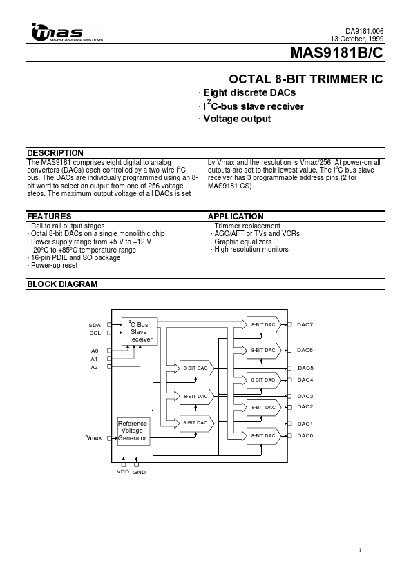
The MAS9181 prises eight digital to analog 2 converters (DACs) each controlled by a two-wire I C bus. The DACs are individually programmed using an 8bit word to select an output from one of 256 voltage steps. The maximum output voltage of all DACs is set
¡¤£¦- ¨- ¨©¨- ¨¤ ¢ !#"%$&(' #()(' 010324)5' 687@9 ACBEDCFE9 G8HPI QPD QSRUTWVUG 68 X Y U ` a E b C c S d 8 d e P f i g q h p 8 h P r 8 h s i g P h p t8u@vCe w f8xEhqvEcCw yCcEw
DA9181.006 13 October, 1999
iCPEEi by Vmax and the resolution is Vmax/256. At power-on all 2 outputs are set to their lowest value. The I C-bus slave receiver has 3 programmable address pins (2 for MAS9181 CS).
dPeif gdCPf hWi
- Rail to rail output stages
- Octal 8-bit DACs on a single monolithic chip
- Power supply range from +5 V to +12 V
- -20°C to +85°C temperature range
- 16-pin PDIL and SO package
- Power-up reset
- Trimmer replacement
- AGC/AFT or TVs and VCRs
- Graphic equalizers
- High resolution monitors jEkml@n
o¨pCq r
sWtPr
u
SDA SCL A0 A1 A2
I C Bus Slave Receiver
{
8-BIT DAC
DAC7
8-BIT DAC
DAC6 DAC5
8-BIT DAC 8-BIT DAC 8-BIT DAC 8-BIT DAC
DAC4 DAC3 DAC2 DAC1 vxwmy z
Reference Voltage Generator
8-BIT DAC 8-BIT DAC
DAC0
VDD GND
1...