PA7540
PA7540 is PA7540 PEEL Array Programmable Electrically Erasable Logic manufactured by Unknown Manufacturer.
- Part of the PA7 comparator family.
- Part of the PA7 comparator family.
features
- Independent or global clocks, resets, presets, clock polarity and output enables
- Sum-of-products logic for output enables Development and Programmer Support
- Anachip’s Win PLACE Development Software
- Fitters for ABEL, CUPL and other software
- Programming support by popular third-party programmers presets, clock polarity, and other features
, making the PA7540 suitable for a variety of binatorial, synchronous and asynchronous logic applications. With pin patibility and super-set functionality to most 24-pin PLDs, (22V10, EP610/630, GAL6002), the PA7540 can implement designs that exceed the architectures of such devices. The PA7540 supports speeds as fast as 10ns/15ns (tpdi/tpdx) and 71.46MHz (f MAX) at moderate power consumption 80m A (55m A typical). Packaging includes 24-pin DIP, SOIC and 28-pin PLCC (see Figure 1). Anachip and popular third-party development tool manufacturers provide development and programming support for the PA7540.
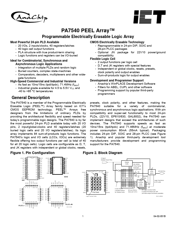
General Description
The PA7540 is a member of the Programmable Electrically Erasable Logic (PEEL™) Array family based on ICT’s CMOS EEPROM technology. PEEL™ Arrays free designers from the limitations of ordinary PLDs by providing the architectural flexibility and speed needed for today’s programmable logic designs. The PA7540 is by far the most powerful 24-pin PLD available today with 20 I/O pins, 2 input/global-clocks and 40 registers/latches (20 buried logic cells and 20 I/O registers/latches). Its logic array implements 84 sum-of-products logic functions. The PA7540’s logic and I/O cells (LCCs, IOCs) are extremely flexible offering two output functions per cell (a total of 40 for all 20 logic cells). Logic cells are configurable as D, T, and JK registers with independent or global clocks, resets,
Figure 1. Pin Configuration
I/C LK1 I/O I/O I/O I/O I/O I/O I/O I/O I/O I/O GND 1 2 3 4 5 6 7 8 9 10 11 12 24 23 22 21 20 19 18 17 16 15 14 13 VC C I/O I/O I/O I/O I/O I/O I/O I/O I/O I/O I/C LK2 I/C LK1 I/O I/O I/O I/O I/O...