QL2009-0PF144C Overview
Key Specifications
Operating Voltage: 3.3 V
Max Voltage (typical range): 3.6 V
Min Voltage (typical range): 3 V
Max Frequency: 130 MHz
Key Features
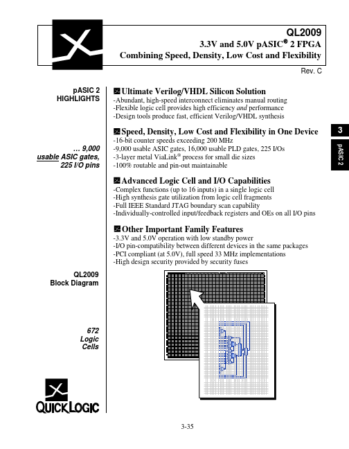
- The QL2009 contains 672 logic cells
- With 225 maximum I/Os, the QL2009 is available in 144-pin TQFP, 208-PQFP, and 256-pin PBGA packages
- Software support for the complete pASIC families, including the QL2009, is available through three basic packages
- The turnkey QuickWorks® pac