QL2003 Overview
Key Specifications
Package: LFQFP
Operating Voltage: 5 V
Max Voltage (typical range): 5.25 V
Min Voltage (typical range): 4.75 V
Key Features
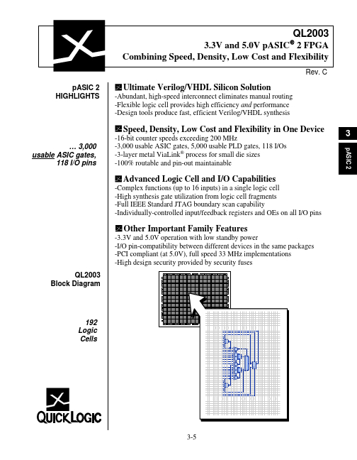
- The QL2003 contains 192 logic cells
- With 118 maximum I/Os, the QL2003 is available in 84-PLCC, 100-pin TQFP and 144-pin TQFP packages
- Software support for the complete pASIC families, including the QL2003, is available through three basic packages