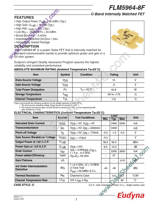
FLM5964-8F
FLM5964-8F is C-Band Internally Matched FET manufactured by Eudyna Devices.
FEATURES
.c
- High Output Power: P1d B = 39.5d Bm (Typ.) U
- High Gain: G1d B = 10.0d B (Typ.) 4 t
- High PAE: ηadd = 37% (Typ.) e = 28.5d Bm
- Low IM3 = -46d Bc@Po e
- Broad Band: 5.9h ~ 6.4GHz S
- Impedance Matched Zin/Zout = 50Ω a Sealed Package t
- Hermetically a DESCRIPTION
D . The FLM5964-8F is a power Ga As FET that is internally matched for w standard munication bands to provide optimum power and gain in a w 50 ohm system.
Item Drain-Source Voltage Gate-Source Voltage Total Power Dissipation Storage Temperature Channel Temperature Symbol VDS VGS PT Tstg Tch Condition
Eudyna’s stringent Quality Assurance Program assures the highest reliability and consistent performance. ABSOLUTE MAXIMUM RATING (Ambient Temperature Ta=25°C)
Tc = 25°C
Fujitsu remends the following conditions for the reliable operation of Ga As FETs: 1. The drain-source operating voltage (VDS) should not exceed 10 volts. 2. The forward and reverse gate currents should not exceed 32.0 and -4.4 m A respectively with gate resistance of 100Ω.
ELECTRICAL CHARACTERISTICS (Ambient Temperature Ta=25°C)
Item Saturated Drain Current Transconductance Pinch-off Voltage Symbol Test Conditions Min. -0.5 -5.0 38.5 VDS =10V, IDS = 0.65IDSS (Typ.), f = 5.9 ~ 6.4 GHz, ZS=ZL= 50 ohm f = 6.4 GHz, ∆f = 10 MHz 2-Tone Test Pout = 28.5d Bm S.C.L. Channel to Case 10V x Idsr x Rth 9.0 -44 Limit Typ. Max. 3400 5200 3400 -1.5 39.5 10.0 37 -46 3.0 -3.0 ±0.6 Unit m A m S V V d Bm d B m A %
Gate Source Breakdown Voltage Output Power at 1d B G.C.P. Power Gain at 1d B G.C.P. Drain Current
Power-added Efficiency Gain Flatness 3rd Order Intermodulation Distortion Thermal Resistance Channel Temperature Rise CASE STYLE: IB w w
.D w
IDSS gm Vp t a
S a e h t e
U 4
Rating 15 -5 42.8
.c
175 m o
Unit V V W °C °C
-65 to +175
VDS = 5V, VGS = 0V VDS = 5V, IDS = 2200m A VDS = 5V, IDS = 170m A IGS = -170µA
VGSO P1d B
G1d B Idsr ηadd ∆G IM3 Rth ∆Tch
2200 2600
G.C.P.: Gain pression Point, S.C.L.: Single Carrier Level
Edition...