Datasheet Summary
.. xr
DECEMBER 2006
INTELLIGENT DYNAMIC CLOCK SWITCH PLL CLOCK DRIVER
REV. 1.0.1
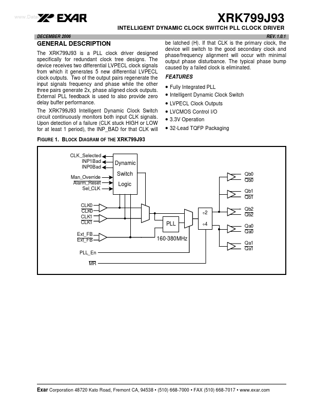
GENERAL DESCRIPTION
The XRK799J93 is a PLL clock driver designed specifically for redundant clock tree designs. The device receives two differential LVPECL clock signals from which it generates 5 new differential LVPECL clock outputs. Two of the output pairs regenerate the input signals frequency and phase while the other three pairs generate 2x, phase aligned clock outputs. External PLL feedback is used to also provide zero delay buffer performance. The XRK799J93 Intelligent Dynamic Clock Switch circuit continuously monitors both input CLK signals. Upon detection of a failure...