EMB09N03G Overview
| Part | EMB09N03G |
|---|---|
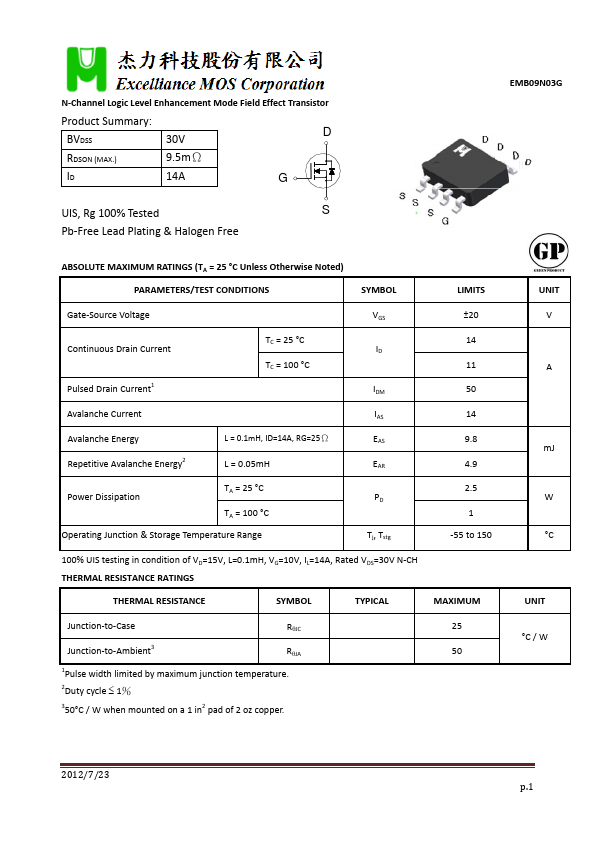
| Description | N-Channel Logic Level Enhancement Mode Field Effect Transistor |
| Category | Transistor |
| Manufacturer | Excelliance MOS |
| Size | 185.80 KB |
| Seller | Inventory | Price Breaks | Buy |
|---|---|---|---|
| UnikeyIC | 400000 | 100+ : 0.1304 USD 200+ : 0.1283 USD 300+ : 0.125 USD |
View Offer |
| Unikeyic (ICkey) | 400000 | 100+ : 0.1304 USD 200+ : 0.1283 USD 300+ : 0.125 USD |
View Offer |
| Part Number | Manufacturer | Description |
|---|---|---|
| BDT88 | Inchange Semiconductor | Silicon PNP Power Transistor |
| KD333 | Tesla Elektronicke | Transistor |
| C828 | SEMTECH | NPN Silicon Transistor |