EMB09N03V Overview
Key Specifications
Min Operating Temp: -55 °C
| Part | EMB09N03V |
|---|---|
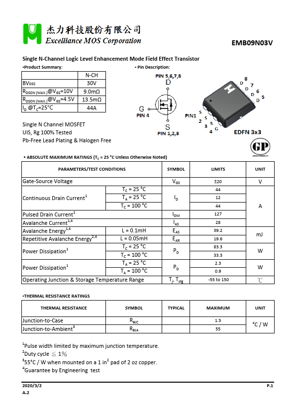
| Description | Single N-Channel Logic Level Enhancement Mode Field Effect Transistor |
| Category | Transistor |
| Manufacturer | Excelliance MOS |
| Size | 446.02 KB |
Min Operating Temp: -55 °C
| Seller | Inventory | Price Breaks | Buy |
|---|---|---|---|
| ICPartonline | 38241 | 1+ : 14 USD 10+ : 13.3 USD 100+ : 12.6 USD 1000+ : 11.9 USD |
View Offer |
| Worldway Electronics | 20816 | 7+ : 0.2133 USD 10+ : 0.209 USD 100+ : 0.2026 USD 500+ : 0.1962 USD |
View Offer |
| Part Number | Manufacturer | Description |
|---|---|---|
| BDT88 | Inchange Semiconductor | Silicon PNP Power Transistor |
| KD333 | Tesla Elektronicke | Transistor |
| C828 | SEMTECH | NPN Silicon Transistor |