EMDJ0N25Q
EMDJ0N25Q is MOSFET manufactured by Excelliance MOS.
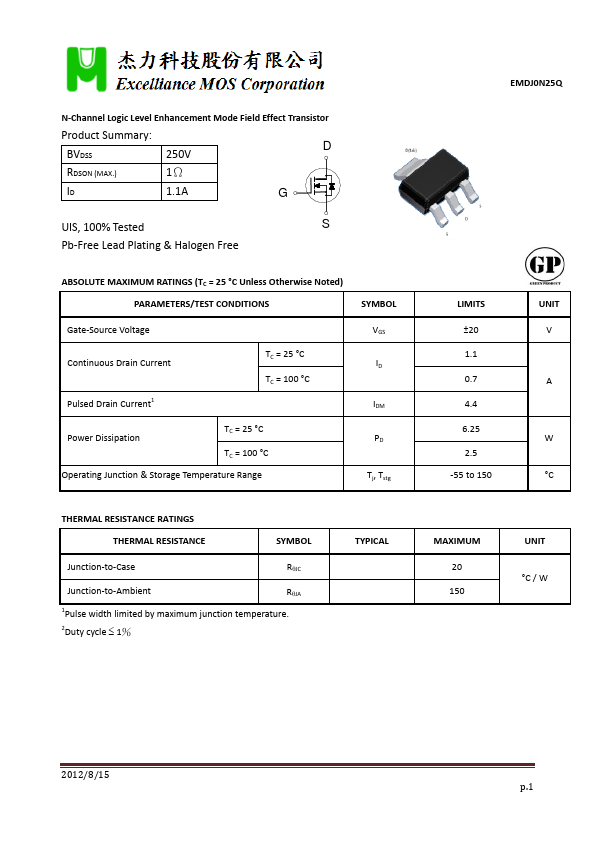
N‐Channel Logic Level Enhancement Mode Field Effect Transistor
Product Summary:
BVDSS
250V
RDSON (MAX.)
1Ω
1.1A
UIS, 100% Tested
Pb‐Free Lead Plating & Halogen Free
ABSOLUTE MAXIMUM RATINGS (TC = 25 °C Unless Otherwise Noted) PARAMETERS/TEST CONDITIONS
SYMBOL
Gate‐Source Voltage
Continuous Drain Current Pulsed Drain Current1
TC = 25 °C TC = 100 °C
Power Dissipation
TC = 25 °C TC = 100 °C
Operating Junction & Storage Temperature Range
VGS ID IDM PD Tj, Tstg
THERMAL RESISTANCE RATINGS THERMAL RESISTANCE
SYMBOL
Junction‐to‐Case
RJC
Junction‐to‐Ambient
RJA
1Pulse width limited by maximum junction temperature. 2Duty cycle 1%
TYPICAL
LIMITS ±20 1.1 0.7 4.4 6.25 2.5
‐55 to 150
UNIT V
W °C
MAXIMUM 20 150
UNIT °C / W
2012/8/15 p.1
ELECTRICAL CHARACTERISTICS (TC = 25 °C, Unless Otherwise Noted)
PARAMETER...