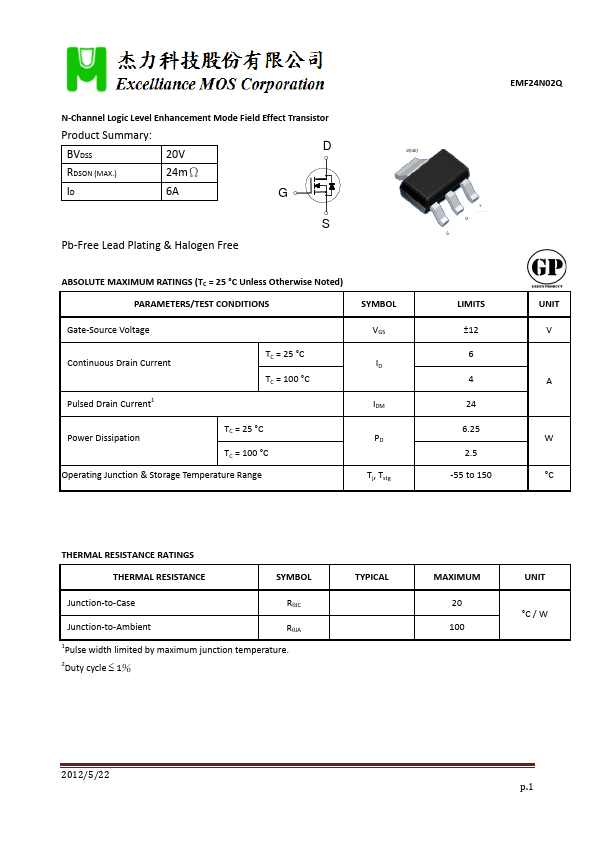
| Part | EMF24N02Q |
|---|---|
| Description | MOSFET |
| Category | MOSFET |
| Manufacturer | Excelliance MOS |
| Size | 223.59 KB |
Pricing from 0.1188 USD, available from UnikeyIC and Unikeyic (ICkey).Powered by Octopart
Price & Availability
| Seller | Inventory | Price Breaks | Buy |
|---|---|---|---|
| UnikeyIC | 400000 | 200+ : 0.1188 USD 400+ : 0.1167 USD 600+ : 0.1138 USD |
View Offer |
| Unikeyic (ICkey) | 400000 | 200+ : 0.1188 USD 400+ : 0.1167 USD 600+ : 0.1138 USD |
View Offer |
Similar Parts
| Part Number | Manufacturer | Description |
|---|---|---|
| HFDOM44P-xxxSx | Hanbit Electronics | 44Pin Flash Disk Module |
| HFDOM40B-xxxSx | Hanbit Electronics | 40Pin Flash Disk Module |
| CP2105 | Silicon Labs | SINGLE-CHIP USB TO DUAL UART BRIDGE |
