The following content is an automatically extracted verbatim text
from the original manufacturer datasheet and is provided for reference purposes only.
View original datasheet text
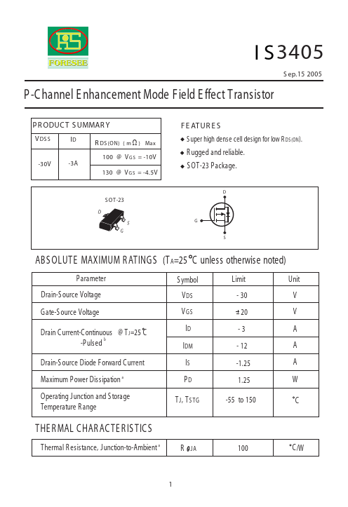
ST I S 3405
S ep.15 2005
P -C hannel E nhancement Mode Field E ffect Transistor
P R ODUC T S UMMAR Y
V DS S ID
-3A
F E AT UR E S
( m W ) Max
R DS (ON)
S uper high dense cell design for low R DS (ON ).
-30V
100 @ V G S = -10V 130 @ V G S = -4.5V
R ugged and reliable. S OT-23 P ackage.
D
S OT-23
D S G
G
S
ABS OLUTE MAXIMUM R ATINGS (T A=25 C unless otherwise noted)
P arameter Drain-S ource Voltage Gate-S ource Voltage Drain C urrent-C ontinuous @ T J =25 C b -P ulsed Drain-S ource Diode Forward C urrent Maximum P ower Dissipation a Operating Junction and S torage Temperature R ange S ymbol V DS V GS ID IDM IS PD T J , T S TG Limit - 30 20 -3 - 12 -1.25 1.