74ALVC16827
Description
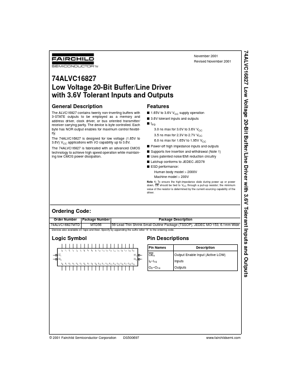
The ALVC16827 contains twenty non-inverting buffers with 3-STATE outputs to be employed as a memory and address driver, clock driver, or bus oriented transmitter/ receiver carrying parity. The device is byte controlled.
Key Features
- Z Outputs O10–O19 L H
- Z H = HIGH Voltage Level L = LOW Voltage Level X = Immaterial (HIGH or LOW, inputs may not float) Z = High Impedance