• Part: 74F174
  • Description: Hex D-Type Flip-Flop with Master Reset
  • Manufacturer: Fairchild Semiconductor
  • Size: 57.44 KB
Download 74F174 Datasheet PDF
Fairchild Semiconductor
74F174
74F174 is Hex D-Type Flip-Flop with Master Reset manufactured by Fairchild Semiconductor.
Description 
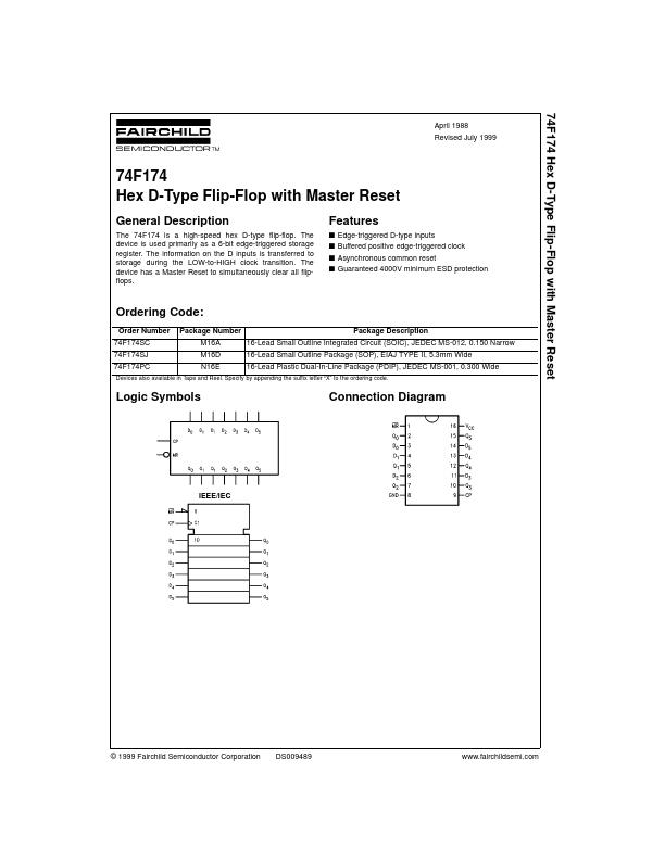
The 74F174 is a high-speed hex D-type flip-flop. The device is used primarily as a 6-bit edge-triggered storage register. The information on the D inputs is transferred to storage during the LOW-to-HIGH clock transition. The device has a Master Reset to simultaneously clear all flipflops. Features s Edge-triggered D-type inputs s Buffered positive edge-triggered clock s Asynchronous mon reset s Guaranteed 4000V minimum ESD protection Ordering Code: Order Number 74F174SC 74F174SJ 74F174PC Package Number M16A M16D N16E Package Description 16-Lead Small Outline Integrated Circuit (SOIC), JEDEC MS-012, 0.150 Narrow 16-Lead Small Outline Package (SOP), EIAJ TYPE II, 5.3mm Wide 16-Lead Plastic Dual-In-Line Package (PDIP), JEDEC MS-001, 0.300 Wide Devices also available in Tape and Reel. Specify by appending the suffix letter “X” to the ordering code. Logic Symbols Connection Diagram IEEE/IEC © 1999 Fairchild Semiconductor Corporation DS009489 .fairchildsemi. Unit Loading/Fan Out Pin Names D0- D5 CP MR Q0- Q5 Data Inputs Clock Pulse Input (Active Rising Edge) Master Reset Input (Active LOW) Outputs Description U.L. HIGH/LOW 1.0/1.0 1.0/1.0 1.0/1.0 50/33.3 Input IIH/IIL Output IOH/IOL 20 µA/- 0.6 m A 20 µA/- 0.6 m A 20 µA/- 0.6 m A - 1 m A/20 m A Functional Description The 74F174 consists of six edge-triggered D-type flip-flops with individual D inputs and Q outputs. The Clock (CP) and Master Reset (MR) are mon to all flip-flops. Each D input’s state is transferred to the corresponding flip-flop’s output following the LOW-to-HIGH Clock (CP) transition. A LOW input to the Master Reset (MR) will force all outputs LOW independent of Clock or Data inputs. The 74F174 is useful for applications where the true output only is required and the Clock and Master Reset are mon to all storage elements. Truth Table Inputs MR L H H CP Dn X H L Outputs Qn L H L H = HIGH Voltage Level L = LOW Voltage Level X = Immaterial = LOW-to-HIGH Clock Transition Logic...