74LCX112
74LCX112 is Low Voltage Dual J-K Negative Edge-Triggered Flip-Flop manufactured by Fairchild Semiconductor.
74LCX112 Low Voltage Dual J-K Negative Edge-Triggered Flip-Flop with 5V Tolerant Inputs
June 1998 Revised February 2001
74LCX112 Low Voltage Dual J-K Negative Edge-Triggered Flip-Flop with 5V Tolerant Inputs
General Description
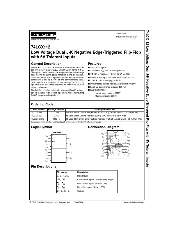
The LCX112 is a dual J-K flip-flop. Each flip-flop has independent J, K, PRESET, CLEAR, and CLOCK inputs with Q, Q outputs. These devices are edge sensitive and change state on the negative going transition of the clock pulse. Clear and preset are independent of the clock and acplished by a low logic level on the corresponding input. LCX devices are designed for low voltage (3.3V or 2.5) operation with the added capability of interfacing to a 5V signal...