74LCX126 Overview
Description
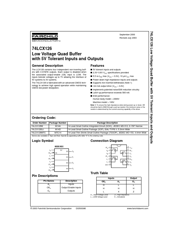
The LCX126 contains four independent non-inverting buffers with 3-STATE outputs. Each output is disabled when the associated output-enable (OE) input is LOW.
Key Features
- Z = High Impedance X = Immaterial © 2003 Fairchild Semiconductor Corporation DS500386 74LCX126