74LCX16244
74LCX16244 is Low Voltage 16-Bit Buffer/Line Driver manufactured by Fairchild Semiconductor.
74LCX16244 Low Voltage 16-Bit Buffer/Line Driver with 5V Tolerant Inputs and Outputs
February 1994 Revised April 1999
74LCX16244 Low Voltage 16-Bit Buffer/Line Driver with 5V Tolerant Inputs and Outputs
General Description
The LCX16244 contains sixteen non-inverting buffers with 3-STATE outputs designed to be employed as a memory and address driver, clock driver, or bus oriented transmitter/receiver. The device is nibble controlled. Each nibble has separate 3-STATE control inputs which can be shorted together for full 16-bit operation. The LCX16244 is designed for low voltage (2.5V or 3.3V) VCC applications with capability of interfacing to a 5V signal environment. The LCX16244 is fabricated with an advanced CMOS technology to achieve high speed operation while maintaining CMOS low power dissipation.
Features s 5V tolerant inputs and outputs s 2.3V- 3.6V VCC specifications provided s 4.5 ns t PD max (VCC = 3.0V), 20 µA ICC max s Power down high impedance inputs and outputs s Supports live insertion/withdrawal (Note 1) s ±24 m A output drive (VCC = 3.0V) s Implements patented noise/EMI reduction circuitry s Latch-up performance exceeds 500 m A s ESD performance: Human body model > 2000V Machine model > 200V
Note 1: To ensure the high-impedance state during power up or down OE should be tied to VCC through a pull-up resistor: the minimum value or the resistor is determined by the current-sourcing capability of the driver.
Ordering Code:
Order Number 74LCX16244MEA 74LCX16244MTD Package Number MS48A MTD48 Package Description 48-Lead Small Shrink Outline Package (SSOP), JEDEC MO-118, 0.300” Wide 48-Lead Thin Shrink Small Outline Package (TSSOP), JEDEC MO-153, 6.1mm Wide
Devices also available in Tape and Reel. Specify by appending the suffix letter “X” to the ordering code.
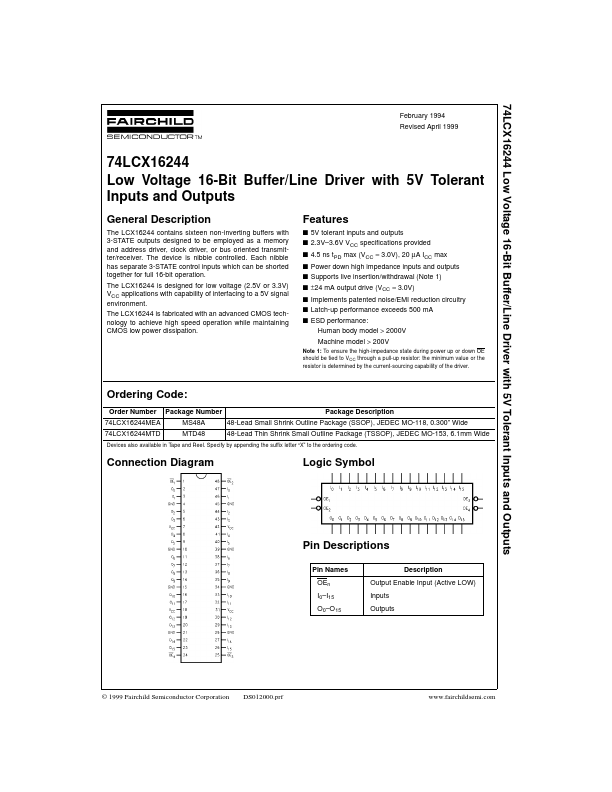
Connection Diagram
Logic Symbol
Pin Descriptions
Pin Names OEn I0- I15 O0- O15 Description Output Enable Input (Active LOW) Inputs Outputs
© 1999 Fairchild Semiconductor Corporation
DS012000.prf...