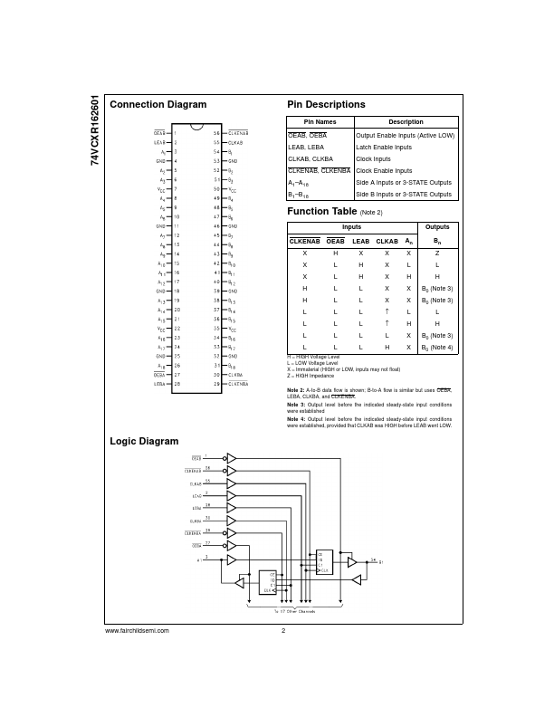
Datasheet4U Logo Datasheet4U.com

74VCXR162601 - Low Voltage 18-Bit Universal Bus Transceivers

This page provides the datasheet information for the 74VCXR162601, a member of the 74VCXR Low Voltage 18-Bit Universal Bus Transceivers family.

Description

The VCXR162601, 18-bit universal bus transceiver, combines D-type latches and D-type flip-flops to allow data flow in transparent, latched, and clocked modes.

Data flow in each direction is controlled by output-enable (OEAB and OEBA), latch-enable (LEAB and LEBA), and clock (CLKAB and CLKBA) inputs.

Features

  • s 1.4V to 3.6V VCC supply operation s 3.6V tolerant inputs and outputs s 26Ω series resistors on both the A and B Port outputs. s tPD (A to B, B to A) 3.8 ns max for 3.0V to 3.6V VCC s Power-down HIGH impedance inputs and outputs s Supports live insertion/withdrawal (Note 1) s Static Drive (IOH/IOL) ±12 mA @ 3.0V VCC s Uses patented noise/EMI reduction circuitry s Latchup performance exceeds 300 mA s ESD performance: Human body model > 2000V Machine model >200V Note 1: To ensure the high-impeda.

📥 Download Datasheet

Datasheet preview – 74VCXR162601

Datasheet Details

Part number 74VCXR162601
Manufacturer Fairchild Semiconductor
File Size 142.96 KB
Description Low Voltage 18-Bit Universal Bus Transceivers
Datasheet download datasheet 74VCXR162601 Datasheet
Additional preview pages of the 74VCXR162601 datasheet.
Other Datasheets by Fairchild Semiconductor

Full PDF Text Transcription

Click to expand full text
74VCXR162601 Low Voltage 18-Bit Universal Bus Transceivers with 3.6V Tolerant Inputs and Outputs and 26Ω Series Resistors in the Outputs August 1998 Revised October 2004 74VCXR162601 Low Voltage 18-Bit Universal Bus Transceivers with 3.6V Tolerant Inputs and Outputs and 26Ω Series Resistors in the Outputs General Description The VCXR162601, 18-bit universal bus transceiver, combines D-type latches and D-type flip-flops to allow data flow in transparent, latched, and clocked modes. Data flow in each direction is controlled by output-enable (OEAB and OEBA), latch-enable (LEAB and LEBA), and clock (CLKAB and CLKBA) inputs. The clock can be controlled by the clock-enable (CLKENAB and CLKENBA) inputs. For A-to-B data flow, the device operates in the transparent mode when LEAB is HIGH.
Published: |