CD4027BCN
Description
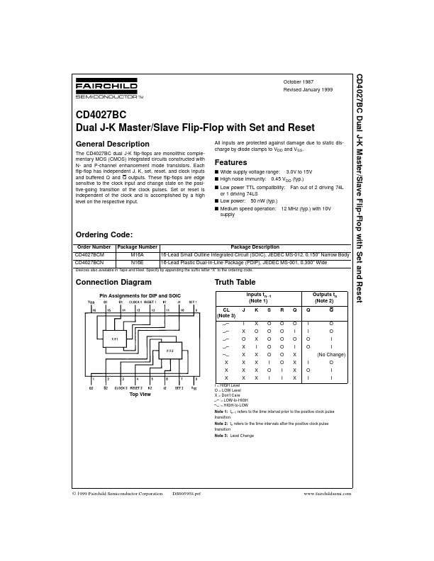
The CD4027BC dual J-K flip-flops are monolithic plementary MOS (CMOS) integrated circuits constructed with N- and P-channel enhancement mode transistors.
Key Features
- Specify by appending the suffix letter “X” to the ordering code
- CD4027BC Logic Diagram .fairchildsemi