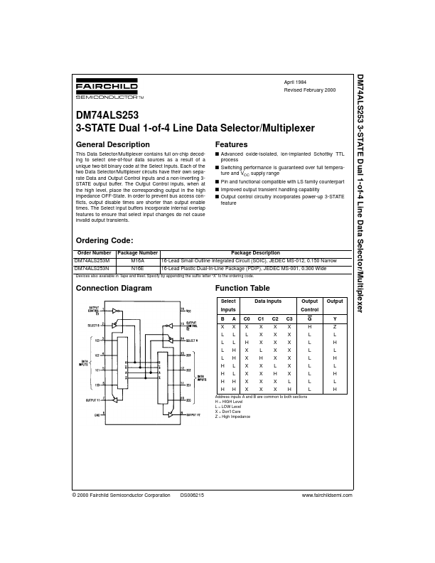
GENERAL DESCRIPTION
The Output Control inputs, when at the high level, place the corresponding output in the high impedance OFF-State. In order to prevent bus access conflicts, output disable times are shorter than output enable times. The Select input buffers incorporate internal overlap features to ensure that select input changes do not cause invalid output transients. FEATURES
s Advanced oxide-isolated, ion-implanted Schottky TTL process s Switching performance is guaranteed over full temperature and VCC supply range s Pin and functional compatible with LS family counterpart s Improved output transient handling capability s Output control circuitry incorporates power-up 3-STATE feature Ordering Code: Order Number DM74ALS253M DM74ALS253N Package Number M16A N16E Package DESCRIPTION
16-Lead Small Outline Integrated Circuit (SOIC), JEDEC MS-012, 0.150 Narrow 16-Lead Plastic Dual-In-Line Package (PDIP), JEDEC MS-001, 0.300 Wide Devices also available in Tape and Reel. Specify by appending the suffix letter “X” to the ordering code. Fairchild Semiconductor