DM74S10 Overview
Description
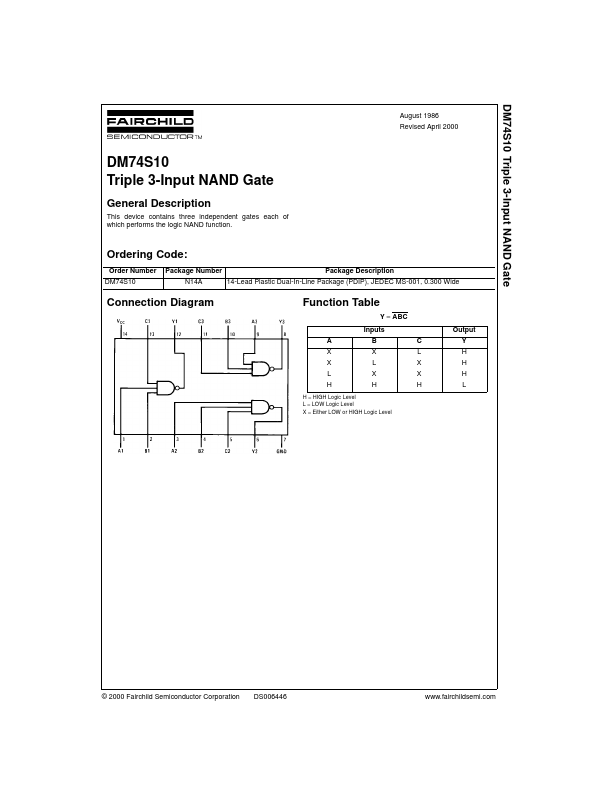
This device contains three independent gates each of which performs the logic NAND function. Ordering Code: Order Number Package Number Package Description DM74S10 N14A 14-Lead Plastic Dual-In-Line Package (PDIP), JEDEC MS-001, 0.300 Wide Connection Diagram Function Table Y = ABC Inputs AB XX XL LX HH H = HIGH Logic Level L = LOW Logic Level X = Either LOW or HIGH Logic Level C L X X H Output Y H H H L © 2000 Fairchild Semiconductor Corporation DS006446 DM74S10 Supply Voltage Input Voltage Operating Free Air Temperature Range Storage Temperature Range 7V 5.5V 0°C to +70°C -65°C to +150°C Note 1: The “ Recommended Operating Conditions Symbol VCC VIH VIL IOH IOL TA Parameter Supply Voltage HIGH Level Input Voltage LOW Level Input Voltage HIGH Level Output Current LOW Level Output Current Free Air Operating Temperature Min 4.75 2 0 Nom 5 Max 5.25 0.8 -1 20 70 Units V V V mA mA °C over recommended operating free air temperature (unless otherwise noted) Symbol Parameter Conditions Min VI Input Clamp Voltage VCC = Min, II = -18 mA VOH HIGH Level Output Voltage VCC = Min, IOH = Max VIL = Max 2.7 VOL LOW Level VCC = Min, IOL = Max Output Voltage VIH = Min II Input Current @ Max Input Voltage VCC = Max, VI = 5.5V IIH HIGH Level Input Current VCC = Max, VI = 2.7V IIL LOW Level Input Current VCC = Max, VI = 0.5V IOS Short Circuit Output Current.