FDC6322C
Description
These dual N & P Channel logic level enhancement mode field effec transistors are produced using Fairchild's proprietary, high cell density, DMOS technology. This very high density process is especially tailored to minimize on-state resistance. The device is an improved design especially for low voltage applications as a replacement for bipolar digital transistors in load switching applications. Since bias resistors are not required, this dual digital FET can replace several digital transistors with difference bias resistors.
Features
N-Ch 25 V, 0.22 A, RDS(ON) = 5 Ω @ VGS= 2.7 V. P-Ch 25 V, -0.46 A, RDS(ON) = 1.5 Ω @ VGS= -2.7 V. Very low level gate drive requirements allowing direct operation in 3 V circuits. VGS(th) < 1.5 V. Gate-Source Zener for ESD ruggedness. >6k V Human Body Model Replace NPN & PNP digital transistors.
SOT-23
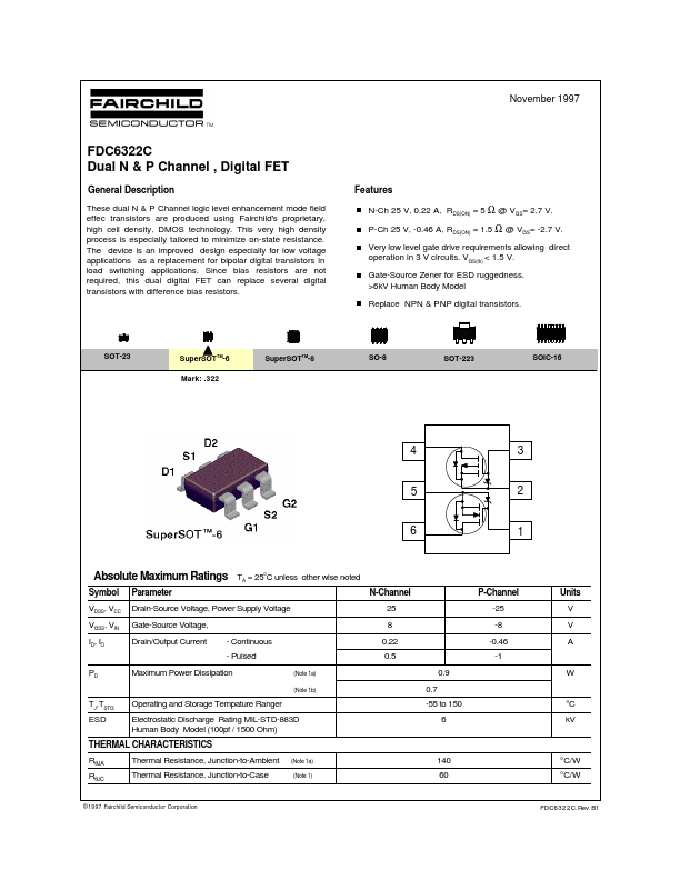
Super SOTTM-6 Mark: .322
Super SOTTM-8
SO-8
SOT-223
SOIC-16
Absolute Maximum Ratings
Symbol VDSS, VCC VGSS, VIN ID, IO...