FDC855N Overview
Key Specifications
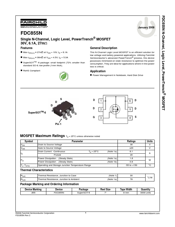
Package: SOT-23-6
Mount Type: Surface Mount
Pins: 6
Height: 1.1 mm
Description
This N-Channel Logic Level MOSFET is an efficient solution for low voltage and battery powered applications. Utilizing Fairchild Semiconductor’s advanced PowerTrench® process, this device possesses minimized on-state resistance to optimize the power consumption.
Key Features
- Max rDS(on) = 27mΩ at VGS = 10V, ID = 6.1A
- Max rDS(on) = 36mΩ at VGS = 4.5V, ID = 5.3A
- SuperSOTTM -6 package: small footprint (72% smaller than standard SO-8; low profile (1mm thick)
- RoHS Compliant tm