Download FDD5N53 Datasheet PDF
Fairchild Semiconductor
FDD5N53
FDD5N53 is N-Channel MOSFET manufactured by Fairchild Semiconductor.
FDD5N53 / FDU5N53 N-Channel MOSFET January 2009 FDD5N53/FDU5N53 N-Channel MOSFET 530V, 4A, 1.5Ω Features - RDS(on) = 1.25Ω ( Typ.)@ VGS = 10V, ID = 2A - Low gate charge ( Typ. 11n C) - Low Crss ( Typ. 5p F) - Fast switching - 100% avalanche tested - Improved dv/dt capability - Ro HS pliant Uni FETTM tm Description 
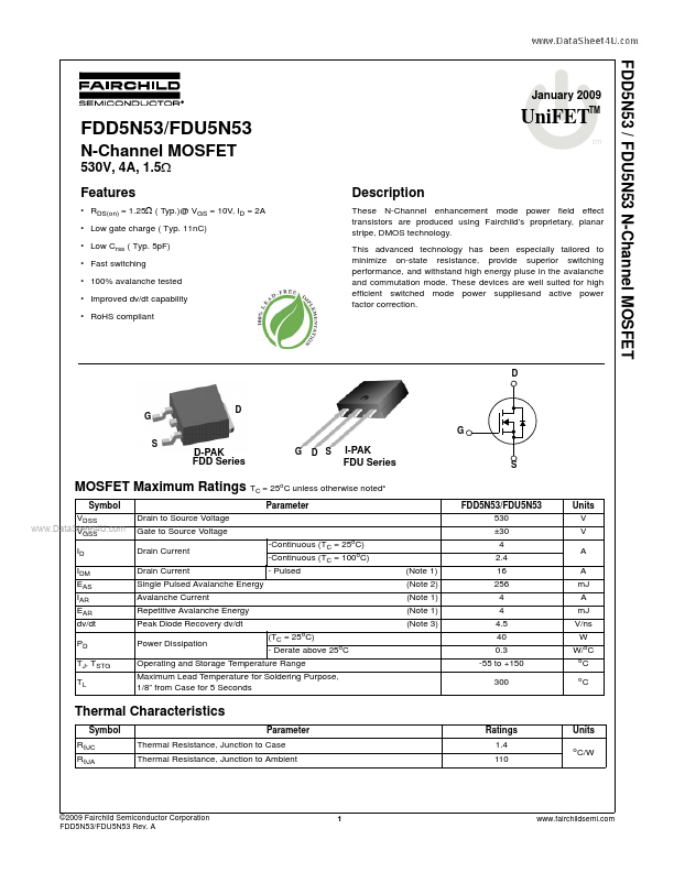
These N-Channel enhancement mode power field effect transistors are produced using Fairchild’s proprietary, planar stripe, DMOS technology. This advanced technology has been especially tailored to minimize on-state resistance, provide superior switching performance, and withstand high energy pluse in the avalanche and mutation mode. These devices are well suited for high efficient switched mode power suppliesand active power factor correction. D-PAK FDD Series I-PAK FDU Series MOSFET Maximum Ratings TC = 25o C unless otherwise noted- Symbol VDSS .. V Parameter Drain to Source Voltage Gate to Source Voltage Drain Current Drain Current Single Pulsed Avalanche Energy Avalanche Current Repetitive Avalanche Energy Peak Diode Recovery dv/dt Power Dissipation (TC = 25o C) - Derate above 25o C -Continuous (TC = 25o C) -Continuous (TC = 100o C) - Pulsed (Note 1) (Note 2) (Note 1) (Note 1) (Note 3) FDD5N53/FDU5N53 530 ±30 4 2.4 16 256 4 4 4.5 40 0.3 -55 to +150 300 Units V V A A m J A m J V/ns W W/o C o o ID IDM EAS IAR EAR dv/dt PD TJ, TSTG TL Operating and Storage Temperature Range Maximum Lead Temperature for Soldering Purpose, 1/8” from Case for 5 Seconds Thermal Characteristics Symbol RθJC RθJA Parameter Thermal Resistance, Junction to Case Thermal Resistance, Junction to Ambient Ratings 1.4 110 Units o C/W ©2009 Fairchild Semiconductor Corporation FDD5N53/FDU5N53 Rev....