FDD6796 Overview
Key Specifications
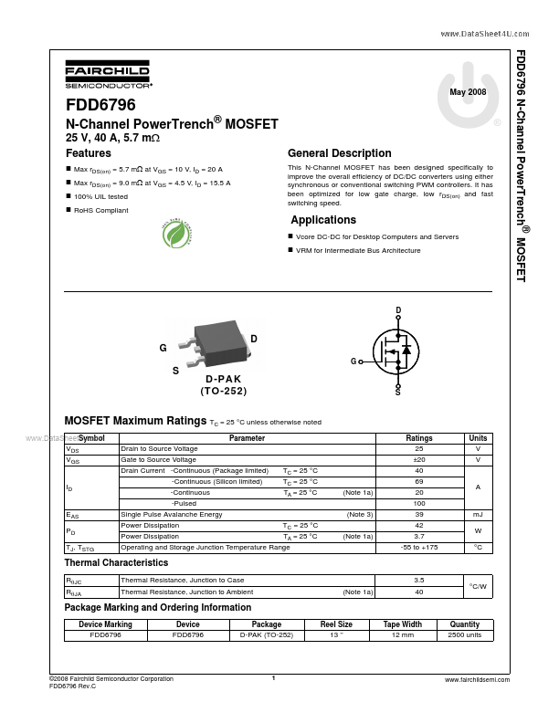
Package: TO-252
Mount Type: Surface Mount
Max Operating Temp: 175 °C
Min Operating Temp: -55 °C
Key Features
- Max rDS(on) = 5.7 mΩ at VGS = 10 V, ID = 20 A
- Max rDS(on) = 9.0 mΩ at VGS = 4.5 V, ID = 15.5 A
| Part | FDD6796 |
|---|---|
| Description | N-Channel MOSFET |
| Category | MOSFET |
| Manufacturer | Fairchild Semiconductor |
| Size | 320.74 KB |
Package: TO-252
Mount Type: Surface Mount
Max Operating Temp: 175 °C
Min Operating Temp: -55 °C
| Seller | Inventory | Price Breaks | Buy |
|---|---|---|---|
| Verical | 6220 | 385+ : 0.9743 USD 500+ : 0.8769 USD 1000+ : 0.8086 USD 10000+ : 0.721 USD |
View Offer |
| Rochester Electronics | 15248 | 100+ : 0.7794 USD 500+ : 0.7015 USD 1000+ : 0.6469 USD 10000+ : 0.5768 USD |
View Offer |
| Part Number | Manufacturer | Description |
|---|---|---|
| AP9563GH | Advanced Power Electronics Corp | P-CHANNEL ENHANCEMENT MODE POWER MOSFET |
| A2SHB | HAOHAI | N-Channel MOSFET |
| FCPF360N65S3R0L | onsemi | N-Channel MOSFET |