FDMC7200S
Features
Q1: N-Channel
- Max r DS(on) = 22 mΩ at VGS = 10 V, ID = 6 A
- Max r DS(on) = 34 mΩ at VGS = 4.5 V, ID = 5 A
Q2: N-Channel
- Max r DS(on) = 10 mΩ at VGS = 10 V, ID = 8.5 A
- Max r DS(on) = 13.5 mΩ at VGS = 4.5 V, ID = 7.2 A
- Ro HS pliant
General Description
This device includes two specialized N-Channel MOSFETs in a dual power33 (3mm X 3mm MLP) package. The switch node has been internally connected to enable easy placement and routing of synchronous buck converters. The control MOSFET (Q1) and synchronous MOSFET (Q2) have been designed to provide optimal power efficiency.
Applications
- Mobile puting
- Mobile Internet Devices
- General Purpose Point of Load
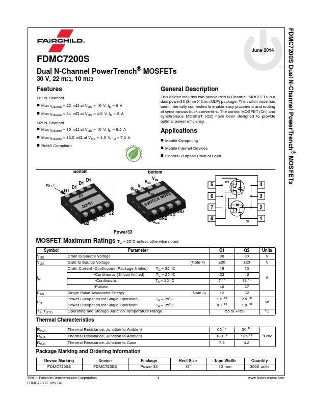
Pin 1
Bottom
D1 D1 D1 G1 D1
D2/S1
S2 S2 S2 G2
Bottom
VIN VIN
GHSVIN
VIN SWITCH
NODE
GND GND GND GLS
5 Q2 6 7 8
4 3 2 1
Q1
Power33
MOSFET Maximum Ratings TC = 25°C unless otherwise noted
Symbol VDS VGS
EAS PD TJ, TSTG
Parameter
Drain to Source Voltage
Gate to Source Voltage
Drain Current -Continuous...