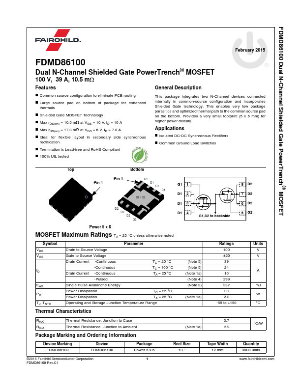
FDMD86100 Description
mon source configuration to eliminate PCB routing Large source pad on bottom of package for enhanced thermals Shielded Gate MOSFET Technology Max rDS(on) = 10.5 mΩ at VGS = 10 V, ID = 10 A Max rDS(on) = 17.3 mΩ at VGS = 6 V, ID = 7.8 A Ideal for flexible layout in secondary side synchronous rectification Termination is Lead-free and RoHS pliant 100% UIL tested This package integrates two N-Channel...
FDMD86100 Key Features
- mon source configuration to eliminate PCB routing
- Large source pad on bottom of package for enhanced thermals
- Shielded Gate MOSFET Technology
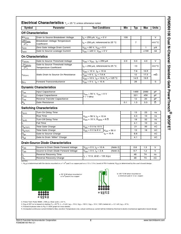
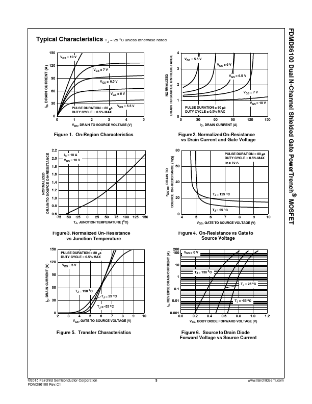
- Max rDS(on) = 10.5 mΩ at VGS = 10 V, ID = 10 A
- Max rDS(on) = 17.3 mΩ at VGS = 6 V, ID = 7.8 A
- Ideal for flexible layout in secondary side synchronous
- Termination is Lead-free and RoHS pliant
- 100% UIL tested